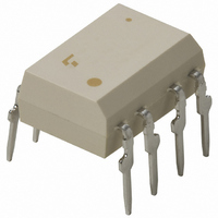
TLP2200 Toshiba, TLP2200 Datasheet - Page 4

TLP2200
Manufacturer Part Number
TLP2200
Description
PHOTOCOUPLER LOGIC OUT 8-DIP
Manufacturer
Toshiba
Specifications of TLP2200
Voltage - Isolation
2500Vrms
Number Of Channels
1, Unidirectional
Current - Output / Channel
25mA
Data Rate
2.5MBd
Propagation Delay High - Low @ If
250ns @ 1.6mA ~ 5mA
Current - Dc Forward (if)
10mA
Input Type
DC
Output Type
Tri-State
Mounting Type
Through Hole
Package / Case
8-DIP (0.300", 7.62mm)
No. Of Channels
1
Isolation Voltage
2.5kV
Optocoupler Output Type
Schmitt Trigger
Input Current
5mA
Output Voltage
20V
Opto Case Style
DIP
No. Of Pins
8
Approval Bodies
UL
Rohs Compliant
Yes
Lead Free Status / RoHS Status
Contains lead / RoHS non-compliant
Available stocks
Company
Part Number
Manufacturer
Quantity
Price
Company:
Part Number:
TLP2200
Manufacturer:
TOS
Quantity:
5 510
Company:
Part Number:
TLP2200
Manufacturer:
TOS
Quantity:
5 510
Part Number:
TLP2200
Manufacturer:
TOSHBIA
Quantity:
20 000
Company:
Part Number:
TLP2200F
Manufacturer:
MICRON
Quantity:
101
Switching Characteristics
(unless otherwise specified, Ta = 0~85°C,V
Propagation delay time to
logic high output level
Propagation delay time to
logic low output level
Output rise time (10-90%)
Output fall time (90-10%)
Output enable time to
logic high
Output enable time to
logic low
Output disable time from
logic high
Output disable time from
logic low
Common mode transient
immunity at logic high
output
Common mode transient
immunity at logic low
output
(*) All typ. values are at Ta = 25°C, V
(Note 4) Duration of output short circuit time should not exceed 10ms.
(Note 5) The t
(Note 6) CM
Characteristic
1.3V point on the leading edge of the output pulse.
The t
1.3V point on the trailing edge of the output pulse.
voltage in the logic low state (V
CM
voltage in the logic high state (V
H
L
pLH
pHL
is the maximum rate of rise of the common mode voltage that can be sustained with the output
is the maximum rate of fall of the common mode voltage that can be sustained with the output
propagation delay is measured from the 50% point on the leading edge of the input pulse to the
propagation delay is measured from the 50% point on the trailing edge of the input pulse to the
(Note 5)
(Note 5)
(Note 6)
(Note 6)
Symbol
CM
CM
t
t
t
t
t
t
pLH
pHL
pZH
pHZ
pZL
pLZ
t
t
r
f
H
L
CC
O
= 5V, I
O
≤ 0.8V).
≤ 2.0V).
Test
Cir-
cuit
1
2
3
F(ON)
CC
4
= 4.5~20V,I
= 3mA unless otherwise specified.
Without peaking capacitor
C
With peaking capacitor C
Without peaking capacitor
C
With peaking capacitor C
I
Ta = 25°C
I
Ta = 25°C
F
F
1
1
= 1.6mA, V
= 0mA, V
Test Condition
CM
CM
―
―
―
―
―
F(ON)
= 50V,
= 50V,
= 1.6~5mA,I
1
1
-1000
1000
Min.
―
―
―
―
―
―
―
―
―
―
F(OFF)
Typ.
235
250
35
20
―
―
―
―
―
―
―
―
= 0~0.1mA)
2002-09-25
Max.
TLP2200
400
400
―
―
―
―
―
―
―
―
―
―
V / µs
V / µs
Unit
ns
ns
ns
ns
ns
ns
ns
ns


