HCPL-3101 Avago Technologies US Inc., HCPL-3101 Datasheet
HCPL-3101
Specifications of HCPL-3101
Available stocks


Related parts for HCPL-3101


HCPL-3101 Summary of contents
Page 1
... The HCPL-3100 switches a 3000 pF load and the HCPL-3101, using a higher speed LED, switches a 3000 pF load in 0.5 s. With a CMR rating of 15 kV/ s typical these opto-couplers readily reject transients found in inverter applications. ...
Page 2
... RoHS compliant. Example 2: HCPL-3101-000E to order product of 300 mil DIP package in Tube packaging and RoHS compliant. Option datasheets are available. Contact your Avago sales representative or authorized distributor for information. Remarks: The notation ‘#XXX’ is used for existing products, while (new) products launched since July 15, 2001 and RoHS compliant will use ‘ ...
Page 3
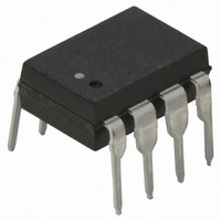
... HCPL-3100 ANODE CATHODE 2 7 GND Q2 3.00 (0.118) 4.00 (0.157 2.55 (0.100) 3.55 (0.140) 0.40 (0.016) 0.60 (0.024 0.16 (0.006) 0.36 (0.014 HCPL-3101 ANODE 2 7 GND CATHODE ...
Page 4
... Through insulation distance conductor to conductor inside the optocoupler cavity Device Min. Max. -55 125 S HCPL-3100 -40 100 HCPL-3101 -40 85 HCPL-3100 25 HCPL-3101 20 HCPL-3100 6 R HCPL-3101 0.1 0.6 35 0.1 0.6 500 O 550 T 270 C for 10 s, 1.0 mm below seating plane Conditions Unit Conditions Fig ...
Page 5
... BYPASS CAPACITOR C = 0.1 F Figure 1. Recommended output transistor protection and typical application circuit. 5 Device Min HCPL-3100 14 F HCPL-3101 15 T -40 A recommended circuit design showing a current limiting resistor R which is necessary in 2 order to prevent damage to the output transistors Q1 and Q2. (See Note 7.) A bypass capacitor ...
Page 6
... Low V O2L Level Voltage Leakage I HCPL-3100 O2L Current HCPL-3101 Supply High I HCPL-3100 CCH Current Level HCPL-3101 Low I CCL Level Low to High I HCPL-3100 FLH Threshold Input HCPL-3101 +85 C, HCPL-3101) unless otherwise specified. A Min. Typ. Max. Units - 1.2 1 0 1.6 1. 1.2 1.5 - ...
Page 7
... Low Output HCPL-3101 Level Rise Time t HCPL-3100 r HCPL-3101 Fall Time t HCPL-3100 f HCPL-3101 Output High |CM | HCPL-3100 H Level Common Mode Transient HCPL-3101 Immunity Output Low | Level Common Mode Transient Immunity Packaging Characteristics Parameter Sym. Input-Output Momentary V ISO Withstand Voltage* Resistance (Input-Output) R I-O Capacitance (Input-Output) ...
Page 8
... CC2 - – O1L + . Figure 3. Test circuit for high level output voltage V O1L + – I O2L Figure 5. Test circuit for leakage current I O2L + Figure 7. Test circuit for – FLH HCPL-3100 GND – O2H + O2H HCPL-3100 GND O1L O1L HCPL-3100 GND and I . CCH CCL ...
Page 9
... Figure 9. Test circuit for and t . PLH PHL -40 - 100 125 AMBIENT TEMPERATURE Figure 11. LED forward current vs. ambient temperature, HCPL-3100 – mA, HCPL-3100 mA, HCPL-3101 F 10 Figure 10. Test circuit for -40 - 100 AMBIENT TEMPERATURE Figure 12. LED forward current vs. ambient temperature, HCPL-3101. HCPL-3100 GND 2 7 – – ...
Page 10
... FORWARD VOLTAGE V (V) F Figure 15. Typical forward current vs. forward voltage, HCPL-3100. 120 110 100 100 FLH SUPPLY VOLTAGE V (V) CC Figure 18. Normalized low to high threshold input current vs. supply voltage, HCPL-3101 CC1 V = -12 V CC2 0.1 0.2 0.3 0.4 0.5 0.6 O OUTPUT CURRENT I ( Figure 21. Typical low level output 1 voltage vs ...
Page 11
... C) A Figure 27. Typical high level output 2 voltage vs. ambient temperature, HCPL-3100 0.1 0.2 0.3 0.4 0.5 0.6 O OUTPUT CURRENT I ( Figure 30. Typical low level output 2 voltage vs. output 2 current, HCPL-3101 SUPPLY VOLTAGE V (V) CC Figure 25. Typical high level output 2 voltage vs. supply voltage, HCPL-3100 NEARLY -0.1 A ...
Page 12
... Figure 34. Typical high level supply current vs. supply voltage, HCPL-3101 2.0 1.5 1.0 0.5 0 -40 - 100 AMBIENT TEMPERATURE Figure 37. Typical high level supply current vs. ambient temperature, HCPL-3100 2.0 1.5 1.0 0.5 0 -40 - 100 AMBIENT TEMPERATURE Figure 40. Typical low level supply current vs. ambient temperature, HCPL-3101. ...
Page 13
... Figure 44. Typical propagation delay time vs. ambient temperature, HCPL-3101. 13 1.0 t PHL PLH 0 3000 0 FORWARD CURRENT I (mA) F Figure 42. Typical propagation delay time vs. forward current, HCPL-3101 3000 1.5 1.0 t PHL 0.5 t PLH 0 -40 - 100 AMBIENT TEMPERATURE Figure 43. Typical propagation delay time vs. ambient temperature, HCPL-3100. ...
Page 14
For product information and a complete list of distributors, please go to our website: Avago, Avago Technologies, and the A logo are trademarks of Avago Technologies Limited in the United States and other countries. Data subject to change. Copyright © ...