TLP2601(F) Toshiba, TLP2601(F) Datasheet - Page 8
TLP2601(F)
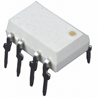
Manufacturer Part Number
TLP2601(F)
Description
PHOTOCOUPLER HS LOGIC OUT 8-DIP
Manufacturer
Toshiba
Specifications of TLP2601(F)
Voltage - Isolation
2500Vrms
Number Of Channels
1, Unidirectional
Current - Output / Channel
25mA
Data Rate
10MBd
Propagation Delay High - Low @ If
60ns @ 7.5mA
Current - Dc Forward (if)
20mA
Input Type
DC
Output Type
Open Collector
Mounting Type
Through Hole
Package / Case
8-DIP (0.300", 7.62mm)
Configuration
1 Channel
Maximum Baud Rate
10 MBd
Maximum Forward Diode Voltage
1.75 V
Maximum Reverse Diode Voltage
5 V
Maximum Power Dissipation
40 mW
Maximum Operating Temperature
+ 70 C
Minimum Operating Temperature
0 C
Isolation Voltage
2500 Vrms
Maximum Continuous Output Current
25 mA
Maximum Fall Time
0.03 us
Maximum Forward Diode Current
20 mA
Output Device
Integrated Photo IC
Lead Free Status / RoHS Status
Lead free / RoHS Compliant
Other names
TLP2601F


Notes
1.
2.
3.
4.
5.
6.
7.
8.
9.
10.
11. Enable
either a ceramic or solid tantalum capacitor with good high frequency characteristic and should be connected
as close as possible to the package V
t
t
t
t
t
t
CM
CM
input
The V
pHL
pLH
f
r
EHL
ELH
L
H
CC
supply voltage to each TLP2601 isolator must be bypassed by a 0.1μF capacitor of larger.This can be
・
・
・
・
・
・
・
・
・
・
Propagation delay is measured from the 3.75mA level on the low to high transition of the input
current pulse to the 1.5V level on the high to low transition of the output voltage pulse.
Propagation delay is measured from the 3.75mA level on the high to low transition of the input
current pulse to the 1.5V level on the low to high transition of the output voltage pulse.
Fall time is measured from the 10% to the 90% levels of the high to low transition on the output
pulse.
Rise time is measured from the 90% to 10% levels of the low to high transition on the output
pulse.
Enable input propagation delay is measured from the 1.5V level on the low to high transition of
the input voltage pulse to the 1.5V level on the high to low transition of the output voltage pulse.
Enable input propagation delay is measured from the 1.5V level on the high to low transition of
the input voltage pulse to the 1.5V level on the low to high transition of the output voltage pulse.
The maximum tolerable rate of fall of the common mode voltage to ensure the output will remain
in the low output state (i.e., V
Measured in volts per microsecond (V / μs).
The maximum tolerable rate of fall of the common mode voltage to ensure the output will remain
in the high state (i.e., V
Measured in volts per microsecond(V / μs).
Volts/microsecond can be translated to sinusoidal voltages:
Example:
V
minimum.
Device considered a two−terminal device: Pins 1, 2, 3 and 4 shorted together, and Pins 5, 6, 7 and
8 shorted together.
No pull up resistor required as the device has an internal pull up resistor.
CM
= 318V
V / μs =
pp
when f
(dv
CM
dt
CM
CC
OUT
)
= 1MHz using CM
Max.
and GND pins of each device.
> 2.0V).
OUT
= f
< 0.8V).
CM
V
8
CM
(p.p.)
L
and CM
H
= 1000V / μs data sheet specified
2007-10-01
TLP2601
Related parts for TLP2601(F)
Image
Part Number
Description
Manufacturer
Datasheet
Request
R

Part Number:
Description:
PHOTOCOUPLER HS LOGIC OUT 8-DIP
Manufacturer:
Toshiba
Datasheet:

Part Number:
Description:
PHOTOCOUPLER HS LOGOUT 8-SMD
Manufacturer:
Toshiba
Datasheet:
Part Number:
Description:
PHOTOCOUPLER HS LOGOUT 8-SMD
Manufacturer:
Toshiba
Datasheet:

Part Number:
Description:
High Speed Optocouplers IC HI SPEED (10Mbps)
Manufacturer:
Toshiba

Part Number:
Description:
Toshiba Semiconductor [TOSHIBA IGBT Module Silicon N Channel IGBT]
Manufacturer:
TOSHIBA Semiconductor CORPORATION
Datasheet:
Part Number:
Description:
TOSHIBA GTR MODULE SILICON NPN TRIPLE DIFFUSED TYPE
Manufacturer:
TOSHIBA Semiconductor CORPORATION
Datasheet:
Part Number:
Description:
TOSHIBA GTR Module Silicon N Channel IGBT
Manufacturer:
TOSHIBA Semiconductor CORPORATION
Datasheet:
Part Number:
Description:
TOSHIBA Intelligent Power Module Silicon N Channel IGBT
Manufacturer:
TOSHIBA Semiconductor CORPORATION
Datasheet:
Part Number:
Description:
TOSHIBA INTELLIGENT POWER MODULE SILICON N CHANNEL LGBT
Manufacturer:
TOSHIBA Semiconductor CORPORATION
Datasheet:
Part Number:
Description:
TOSHIBA IGBT Module Silicon N Channel IGBT
Manufacturer:
TOSHIBA Semiconductor CORPORATION
Datasheet:
Part Number:
Description:
TOSHIBA GTR MODULE SILICON N−CHANNEL IGBT
Manufacturer:
TOSHIBA Semiconductor CORPORATION
Datasheet:
Part Number:
Description:
TOSHIBA Intelligent Power Module Silicon N Channel IGBT
Manufacturer:
TOSHIBA Semiconductor CORPORATION
Datasheet:
Part Number:
Description:
TOSHIBA GTR Module Silicon N Channel IGBT
Manufacturer:
TOSHIBA Semiconductor CORPORATION
Datasheet:
Part Number:
Description:
TOSHIBA INTELLIGENT POWER MODULE
Manufacturer:
TOSHIBA Semiconductor CORPORATION
Datasheet:
Part Number:
Description:
TOSHIBA Intelligent Power Module Silicon N Channel IGBT
Manufacturer:
TOSHIBA Semiconductor CORPORATION
Datasheet: