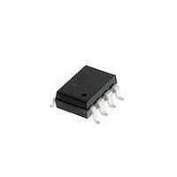
HCPL-5121-300 Avago Technologies US Inc., HCPL-5121-300 Datasheet - Page 15

HCPL-5121-300
Manufacturer Part Number
HCPL-5121-300
Description
ISOLAT 1.5KVDC 1CH TOTEM 8SMD GW
Manufacturer
Avago Technologies US Inc.
Datasheet
1.HCPL-5120.pdf
(16 pages)
Specifications of HCPL-5121-300
Output Type
Push-Pull, Totem-Pole
Package / Case
8-SMD Gull Wing
Voltage - Isolation
1500VDC
Number Of Channels
1, Unidirectional
Current - Output / Channel
2A
Propagation Delay High - Low @ If
300ns @ 10mA ~ 18mA
Current - Dc Forward (if)
25mA
Input Type
DC
Mounting Type
Surface Mount
Configuration
1 Channel
Maximum Propagation Delay Time
500 ns
Maximum Forward Diode Voltage
1.8 V
Minimum Forward Diode Voltage
1.2 V
Maximum Reverse Diode Voltage
5 V
Maximum Forward Diode Current
18 mA
Maximum Power Dissipation
295 mW
Maximum Operating Temperature
+ 125 C
Minimum Operating Temperature
- 55 C
Lead Free Status / RoHS Status
Contains lead / RoHS non-compliant
IPM Dead Time and Propagation Delay Specifications.
The HCPL-520 includes a Propagation Delay Difference
(PDD) specification intended to help designers mini-
mize “dead time” in their power inverter designs. Dead
time is the time period during which both the high and
low side power transistors (Q and Q2 in Figure 25) are
off. Any overlap in Q and Q2 conduction will result in
large currents flowing through the power devices be-
tween the high and low voltage motor rail.
To minimize dead time in a given design, the turn on of
LED2 should be delayed (relative to the turn off of LED)
so that under worst-case conditions, transistor Q has
just turned off when transistor Q2 turns on, as shown in
Figure 33. The amount of delay necessary to achieve this
conditions is equal to the maximum value of the propa-
gation delay difference specification, PDD
specified to be 350 ns over the operating temperature
range of -55°C to 25°C.
Figure 33. Minimum LED Skew for Zero Dead Time
Figure 35. Input Thermal Derating Curve,
Dependence of case-to-ambient Thermal Resistance
5
V OUT1
V OUT2
I LED1
I LED2
20
50
40
30
10
0
-55
case-to-ambient thermal resistance
-25
T
A
- AMBIENT TEMPERATURE -
5
PDD* MAX = (t
= 70
= 140
= 210
t
PHL MAX
Q2 OFF
Q1 ON
35
o
C/W
o
o
C/W
C/W
PHL
t
65
PLH MIN
- t
PLH
)
MAX
95
= t
o
C
PHL MAX
- t
125
Q1 OFF
Q2 ON
PLH MIN
*PDD = PROPAGATION
DELAY DIFFERENCE
NOTE:
FOR PDD CALCULATIONS
THE PROPAGATION DELAYS
ARE TAKEN AT THE SAME
TEMPERATURE AND TEST
CONDITIONS.
MAX
, which is
Delaying the LED signal by the maximum propagation
delay difference ensures that the minimum dead time is
zero, but it does not tell a designer what the maximum
dead time will be. The maximum dead time is equivalent
to the difference between the maximum and minimum
propagation delay difference specifications as shown in
Figure 34. The maximum dead time for the HCPL-520 is
00 ns (= 350 ns - (-350 ns)) over an operating tempera-
ture range of -55°C to 25°C.
Note that the propagation delays used to calculate PDD
and dead time are taken at equal temperatures and test
conditions since the optocouplers under consideration
are typically mounted in close proximity to each other
and are switching identical IGBTs.
Figure 34. Waveforms for Dead Time Calculations
Figure 36. Output Thermal Derating Curve,
Dependence of case-to-ambient Thermal Resistance
V
V
I
I
LED1
OUT1
OUT2
LED2
300
250
200
150
100
50
0
-55
case-to-ambient thermal resistance
-25
T
A
- AMBIENT TEMPERATURE -
(t
= PDD* MAX
Q2 OFF
Q1 ON
t
PHL
PHL MIN
t
PHL MAX
5
- t
PLH
) MAX
= 70
= 140
= 210
35
MAXIMUM DEAD TIME
(DUE TO OPTOCOUPLER)
= (t
= (t
= PDD* MAX - PDD* MIN
o
C/W
o
o
t
C/W
C/W
PLH MIN
PHL MAX
PHL MAX
65
t
PLH MAX
- t
- t
PHL MIN
PLH MIN
95
o
C
) + (t
) - (t
PHL MIN
PLH MAX
125
- t
- t
Q1 OFF
Q2 ON
PLH MAX
PLH MIN
)
)
*PDD = PROPAGATION
DELAY DIFFERENCE
NOTE:
FOR DEAD TIME AND
PDD CALCULATIONS ALL
PROPAGATION DELAYS ARE
TAKEN AT THE SAME
TEMPERATURE AND TEST
CONDITIONS.


