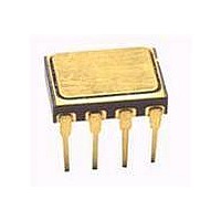
HCPL-5151 Avago Technologies US Inc., HCPL-5151 Datasheet - Page 7

HCPL-5151
Manufacturer Part Number
HCPL-5151
Description
OPTOCOUPLER 0.5A IGBT 8DIP
Manufacturer
Avago Technologies US Inc.
Datasheet
1.HCPL-5150.pdf
(16 pages)
Specifications of HCPL-5151
Output Type
Push-Pull, Totem-Pole
Package / Case
8-CDIP (0.300", 7.62mm)
Voltage - Isolation
1500VDC
Number Of Channels
1, Unidirectional
Current - Output / Channel
400mA
Propagation Delay High - Low @ If
300ns @ 10mA ~ 18mA
Current - Dc Forward (if)
25mA
Input Type
DC
Mounting Type
Through Hole
Configuration
1 Channel
Maximum Propagation Delay Time
500 ns
Maximum Forward Diode Voltage
1.8 V
Minimum Forward Diode Voltage
1.2 V
Maximum Reverse Diode Voltage
5 V
Maximum Forward Diode Current
18 mA
Maximum Power Dissipation
295 mW
Maximum Operating Temperature
+ 125 C
Minimum Operating Temperature
- 55 C
Lead Free Status / RoHS Status
Contains lead / RoHS non-compliant
Package Characteristics
Over recommended operating conditions (T
*All typicals at T
Notes:
1. Maximum pulse width = 10 ms, maximum duty cycle = 0.2%. This value is intended to allow for component tolerances for designs with I
2. Maximum pulse width = 50 ms, maximum duty cycle = 0.5%.
3. In this test V
4. Maximum pulse width = 1 ms, maximum duty cycle = 20%.
5. This is a momentary withstand test, not an operating condition.
6. Device considered a two-terminal device: pins on input side shorted together and pins on output side shorted together.
7. The difference between t
8. Pins 1 and 4 need to be connected to LED common.
9. Common mode transient immunity in the high state is the maximum tolerable |dV
10. Common mode transient immunity in a low state is the maximum tolerable |dV
11. This load condition approximates the gate load of a 1200 V/25 A IGBT.
12. Pulse Width Distortion (PWD) is defined as |t
13. Standard parts receive 100% testing at 25°C (Subgroups 1 and 9). SMD and Class H parts receive 100% testing at 25, 125 and -55°C (Subgroups 1
14. Parameters are tested as part of device initial characterization and after design and process changes. Parameters are guaranteed to limits
7
Parameter
Input-Output Leakage Current
Resistance (Input-Output)
Capacitance (Input-Output)
minimum = 0.5 A. See Applications section for additional details on limiting I
output will remain in the high state (i.e., V
will remain in a low state (i.e., V
and 9, 2 and 10, 3 and 11, respectively).
specified for all lots not specifically tested.
A
OH
= 25°C.
is measured with a dc load current. When driving capacitive loads V
PHL
and t
O
Symbol
< 1.0 V).
R
C
PLH
I
I-O
I-O
I-O
between any two HCPL-5150 parts under the same test condition.
O
V
> 15.0 V).
I-O
PHL
t = 5 sec., T
= 500Vdc RH ≤ 65%,
Test Conditions
-t
V
PLH
I-O
f = MHz
A
| for any given device.
= 500 VDC
= -55 to +125°C) unless otherwise specified.
A
= 5°C
Subgroups
Group A
(13)
OH
peak.
CM
/dt| of the common mode pulse, V
OH
CM
will approach V
Min.
/dt| of the common mode pulse, V
Limits
Typ.
0
.34
0
CC
as I
Max.
.0
OH
approaches zero amps.
Units
mA
W
pF
CM
, to assure that the output
CM
Fig.
, to assure that the
Note
5, 6
6
6
O
peak


