5962-8947701XA Avago Technologies US Inc., 5962-8947701XA Datasheet - Page 7
5962-8947701XA
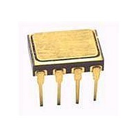
Manufacturer Part Number
5962-8947701XA
Description
OPTOCOUPLER DET AC/DC SLD GW
Manufacturer
Avago Technologies US Inc.
Datasheet
1.HCPL-5760.pdf
(10 pages)
Specifications of 5962-8947701XA
Package / Case
8-SMD Gull Wing
Voltage - Isolation
1500VDC
Number Of Channels
1, Unidirectional
Current - Output / Channel
40mA
Data Rate
100KHz
Propagation Delay High - Low @ If
4µs
Current - Dc Forward (if)
15mA
Input Type
Logic
Output Type
Open Collector
Mounting Type
Surface Mount
Logic Gate Type
AC/DC to Logic Interface Optocouplers
Configuration
1 Channel
Maximum Forward Diode Voltage
0.73 V
Maximum Continuous Output Current
40 mA
Maximum Power Dissipation
260 mW
Maximum Operating Temperature
+ 125 C
Minimum Operating Temperature
- 55 C
Lead Free Status / RoHS Status
Contains lead / RoHS non-compliant


Typical Characteristics All typical values are at T
Notes:
7
1. Maximum operating frequency is defined
2. Measured at a point 1.6 mm below seating
3. Current into/out of any single lead.
4. Surge input current duration is 3 ms at 120
5. Derate linearly above 100 C free-air
6. The 1.8 k load represents 1 TTL unit load
7. Logic low output level at Pin 6 occurs
Parameter
Hysteresis
Input Clamp Voltage
Bridge Diode
Forward Voltage
Input-Output Resistance
Input-Output Capacitance
Input Capacitance
Output Rise Time
(10-90%)
Output Fall Time
(90-10%)
when output waveform (Pin 6) attains only
90% of V
using a 5 V square wave input signal.
plane.
Hz pulse repetition rate. Transient input
current duration is 10 s at 120 Hz pulse
repetition rate. Note that maximum input
power, P
temperature at a rate of 4.26 mW/ C.
Maximum input power dissipation of 195
mW allows an input IC junction
temperature of 150 C at an ambient
temperature of T
thermal resistance from junction to
ambient of
thermal resistance from junction to case is
equal to 170 C/W. Excessive P
may result in device degradation.
of 1.6 mA and the 4.7 k pull-up resistor.
IN
CC
, must be observed.
with R
JAi
= 235 C/W. The typical
A
L
= 125 C with a typical
= 1.8 k , C
L
IN
= 15 pF
and T
J
Symbol
V
V
V
I
V
R
C
C
HYS
D1,2
D3,4
t
t
HYS
ILC
I-O
I-O
IN
r
f
10. This is a momentary withstand test, not an
11. The t
12. The t
13. Common mode transient immunity in Logic
8. The ac voltage is instantaneous voltage.
9. Device considered a two terminal device:
under the conditions of V
as the range of V
exceeded V
Pin 6 occurs under the conditions of V
V
once V
Pins 1, 2, 3, 4 connected together, Pins 5,
6, 7 8 connected together.
operating condition.
from the 2.5 V level of the leading edge of
a 5.0 V input pulse (1 s rise time) to the
1.5 V level on the leading edge of the
output pulse (see Figure 7).
from the 2.5 V level of the trailing edge of a
5.0 V input pulse (1 s fall time) to the 1.5
V level on the trailing edge of the output
pulse (see Figure 7).
High level is the maximum tolerable dV
dt
ensure that the output will remain in a
Logic High state (i.e., V
mode transient immunity in Logic Low
TH-
of the common mode voltage, V
A
as well as the range of V
PHL
PLH
= 25 C, V
-0.76
IN
Typ.
0.62
0.73
10
1.2
1.1
2.0
0.5
50
10
propagation delay is measured
propagation delay is measured
has decreased below V
12
TH+
. Logic high output level at
IN
CC
Units
mA
> V
pF
pF
= 5 V, unless otherwise specified.
V
V
s
s
TH
O
> 2.0 V). Common
IN
– once V
IN
V
Conditions
I
V
V
I
I
V
f = 1 MHz, V
f = 1 MHz; V
Pins 2 & 3, Pins 1 & 4 Open
HYS
IN
IN
TH+
HYS
ILC
I-O
< V
TH-
= -10 mA
= 3 mA (see schematic)
CM
IN
= I
= 500 Vdc
= V
as well
TH+
.
= V
, to
has
TH+
IN
2
CM/
TH+
- V
- I
- V
TH-
3
; V
I-O
IN
TH-
= 0 V,
3
= 0 Vdc
14. In applications where dV
15. D
16. Standard parts receive 100% testing at
17. Parameters shall be tested as part of
= GND;
level is the maximum tolerable dV
the common mode voltage, V
that the output will remain in a Logic Low
state (i.e., V
50,000 V/ s (such as static discharge), a
series resistor, R
protect the detector IC from destructively
high surge currents. The recommended
value for R
drop in V
minimum value of 240 .
are zener diodes.
25 C (Subgroups 1 and 9). SMD,
Class H and Class K parts receive 100%
testing at 25, 125, and -55 C (Subgroups 1
and 9, 2 and 10 ,3 and 11, respectively.)
device initial characterization and after
process changes. Parameters shall be
guaranteed to the limits specified for all
lots not specifically tested.
1
and D
2
CC
are Schottky diodes; D
CC
(between Pin 8 and V
O
is 240
< 0.8 V). See Figure 8.
CC
, should be included to
per volt of allowable
Fig.
CM/dt
1
7
7
CM
may exceed
, to ensure
3
CC
CM/dt
Note
and D
) with a
9
of
4
Related parts for 5962-8947701XA
Image
Part Number
Description
Manufacturer
Datasheet
Request
R

Part Number:
Description:
IC OPAMP GP 600KHZ LP TO99-8
Manufacturer:
Analog Devices Inc
Datasheet:

Part Number:
Description:
OPTOCOUPLER HERMETIC 8-DIP
Manufacturer:
Avago Technologies US Inc.
Datasheet:

Part Number:
Description:
OPTOCOUPLER HERMETIC 8-DIP GW
Manufacturer:
Avago Technologies US Inc.
Datasheet:

Part Number:
Description:
Analog Multiplexer Single 8:1 16-Pin CDIP
Manufacturer:
Intersil
Datasheet:

Part Number:
Description:
ADC Single Semiflash 400KSPS 8-Bit Parallel 24-Pin CDIP
Manufacturer:
Maxim Integrated Products
Datasheet:
Part Number:
Description:
Analog Multiplexer Single 8:1 16-Pin CDIP
Manufacturer:
Maxim Integrated Products
Datasheet:
Part Number:
Description:
Analog Multiplexer Dual 8:1 28-Pin CDIP
Manufacturer:
Intersil
Datasheet:
Part Number:
Description:
CDIP 8/M�/Precision CMOS Analog Switch
Manufacturer:
Maxim Integrated Products

Part Number:
Description:
SPLD, PALCE16V8 Family, EECMOS Process, 300 Gates, 8 Macro Cells, 8 Reg., 8 User I/Os, 5V Supply, 15 Speed Grade, 20DIP
Manufacturer:
Cypress Semiconductor Corporation.
Datasheet:
Part Number:
Description:
OPTOCOUPLER MOSFET HERM 8DIP
Manufacturer:
Avago Technologies US Inc.
Datasheet:
Part Number:
Description:
OPTOCOUPLER GATE HERM SEAL 8DIP
Manufacturer:
Avago Technologies US Inc.
Datasheet:
Part Number:
Description:
OPTOCOUPLER GATE HERM SEAL 8DIP
Manufacturer:
Avago Technologies US Inc.
Datasheet:
Part Number:
Description:
OPTOCOUPLER GATE HERM SEAL 8DIP
Manufacturer:
Avago Technologies US Inc.
Datasheet:

Part Number:
Description:
ADC, LC2MOS High Speed 4-and 8-Channel 8-Bit ADCs
Manufacturer:
Analog Devices
Part Number:
Description:
ADC, LC2MOS High Speed 4-and 8-Channel 8-Bit ADCs
Manufacturer:
Analog Devices