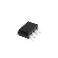
HCPL-5301#300 Avago Technologies US Inc., HCPL-5301#300 Datasheet - Page 9

HCPL-5301#300
Manufacturer Part Number
HCPL-5301#300
Description
ISOLAT 1.5KVDC 1CH OPEN 8SMD GW
Manufacturer
Avago Technologies US Inc.
Datasheet
1.HCPL-5300.pdf
(16 pages)
Specifications of HCPL-5301#300
Output Type
Open Collector
Package / Case
8-SMD Gull Wing
Voltage - Isolation
1500VDC
Number Of Channels
1, Unidirectional
Current - Output / Channel
15mA
Data Rate
2MBd
Propagation Delay High - Low @ If
180ns @ 10mA
Current - Dc Forward (if)
25mA
Input Type
DC
Mounting Type
Surface Mount
Logic Gate Type
Power Module and Gate Drive Interface Optocouplers
Configuration
1 Channel
Current Transfer Ratio
90 %
Maximum Propagation Delay Time
750 ns
Maximum Forward Diode Voltage
1.8 V
Minimum Forward Diode Voltage
1 V
Maximum Reverse Diode Voltage
5 V
Maximum Forward Diode Current
20 mA
Maximum Continuous Output Current
15 mA
Maximum Power Dissipation
145 mW
Maximum Operating Temperature
+ 125 C
Minimum Operating Temperature
- 55 C
Lead Free Status / RoHS Status
Contains lead / RoHS non-compliant
Available stocks
Company
Part Number
Manufacturer
Quantity
Price
developed across the resistor is less than V
will remain off and no common mode failure will occur.
Even if the LED momentarily turns on, the 100 pF capacitor
from pins 6-5 will keep the output from dipping below
the threshold. The recommended LED drive circuit (Figure
13) provides about 10 V of margin between the lowest
optocoupler output voltage and a 3 V IPM threshold during
a 10 kV/ s transient with V
can be obtained by adding a diode in parallel with the
resistor, as shown by the dashed line connection in Figure
18, to clamp the voltage across the LED below V
Since the open collector drive circuit, shown in Figure 19,
cannot keep the LED off during a +dV
not desirable for applications requiring ultra high CMR
performance. Figure 20 is the AC equivalent circuit for
Figure 16 during common mode transients. Essentially all
the current flowing through C
transient must be supplied by the LED. CMR
occur at dv/dt rates where the current through the LED
and C
alternative drive circuit which does achieve ultra high CMR
performance by shunting the LED in the off state.
IPM Dead Time and Propagation Delay Specifications
These devices include a Propagation Delay Difference
specification intended to help designers minimize “dead
time” in their power inverter designs. Dead time is the
time period during which both the high and low side
power transistors (Q1 and Q2 in Figure 22) are off. Any
overlap in Q1 and Q2 conduction will result in large
currents flowing through the power devices between the
high and low voltage motor rails.
To minimize dead time the designer must consider the
propagation delay characteristics of the optocoupler as
well as the characteristics of the IPM IGBT gate drive circuit.
9
LEDN
exceeds the input threshold. Figure 21 is an
CM
= 1000 V. Additional margin
LEDN
during a +dV
CM/dt
transient, it is
F(OFF)
H
failures can
F(OFF)
the LED
.
CM/dt
H
Considering only the delay characteristics of the
optocoupler (the characteristics of the IPM IGBT gate
drive circuit can be analyzed in the same way) it is
important to know the minimum and maximum turn-
on (t
cations, preferably over the desired operating
temperature range.
The limiting case of zero dead time occurs when the
input to Q1 turns off at the same time that the input to
Q2 turns on. This case determines the minimum delay
between LED1 turn-off and LED2 turn-on, which is
related to the worst case optocoupler propagation
delay waveforms, as shown in Figure 23. A minimum
dead time of zero is achieved in Figure 23 when the
signal to turn on LED2 is delayed by (t
from the LED1 turn off. This delay is the maximum
value for the propagation delay difference specification
which is specified at 500 ns for the HCPL-530X over an
operating temperature range of -55 C to +125 C.
Delaying the LED signal by the maximum propagation
delay difference ensures that the minimum dead time
is zero, but it does not tell a designer what the
maximum dead time will be. The maximum dead time
occurs in the highly unlikely case where one opto-
coupler with the fastest t
slowest t
dead time in this case becomes the sum of the spread
in the t
Figure 24. The maximum dead time is also equivalent
to the difference between the maximum and minimum
propagation delay difference specifications. The
maximum dead time (due to the optocouplers) for the
HCPL-530X is 670 ns (= 500 ns - (-170 ns)) over an
operating temperature range of -55 C to +125 C.
PHL
) and turn-off (t
PLH
PHL
and t
are in the same inverter leg. The maximum
PHL
propagation delays as shown in
PLH
) propagation delay specifi-
PLH
and another with the
PLH max
- t
PHL min
)


