HCPL-6630 Avago Technologies US Inc., HCPL-6630 Datasheet - Page 11
HCPL-6630
Manufacturer Part Number
HCPL-6630
Description
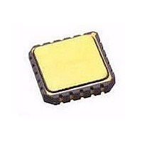
OPTOCOUPLER 10MBS 2CH 20-LCCC
Manufacturer
Avago Technologies US Inc.
Datasheet
1.HCPL-5600.pdf
(12 pages)
Specifications of HCPL-6630
Package / Case
20-LCCC
Voltage - Isolation
1500VDC
Number Of Channels
2, Unidirectional
Current - Output / Channel
25mA
Data Rate
10Mbps
Propagation Delay High - Low @ If
55ns @ 13mA
Current - Dc Forward (if)
20mA
Input Type
DC
Output Type
Open Collector
Mounting Type
Surface Mount
Maximum Continuous Output Current
25 mA
Maximum Fall Time
40 ns
Maximum Forward Diode Current
20 mA
Maximum Rise Time
90 ns
Output Device
Logic Gate Photo IC
Configuration
2 Channel
Maximum Baud Rate
10 MBps
Maximum Forward Diode Voltage
1.9 V
Maximum Reverse Diode Voltage
5 V
Maximum Power Dissipation
200 mW
Maximum Operating Temperature
+ 125 C
Minimum Operating Temperature
- 55 C
Number Of Elements
2
Baud Rate
10Mbps
Forward Voltage
1.9V
Forward Current
20mA
Output Current
25mA
Package Type
LCCC
Operating Temp Range
-55C to 125C
Fall Time
40ns
Rise Time
90ns
Power Dissipation
200mW
Propagation Delay Time
140ns
Pin Count
20
Mounting
Surface Mount
Reverse Breakdown Voltage
5V
Operating Temperature Classification
Military
Lead Free Status / RoHS Status
Lead free by exemption / RoHS compliant by exemption
Lead Free Status / RoHS Status
Lead free / RoHS Compliant, Lead free by exemption / RoHS compliant by exemption
Available stocks
Company
Part Number
Manufacturer
Quantity
Price
Company:

Part Number:
HCPL-6630
Manufacturer:
AVAGO
Quantity:
1 400


Figure 8. Test Circuit for t
Figure 10. Operating Circuit for Burn-In and Steady State Life Tests.
11
GENERATOR
Z
I
CONDITIONS: I
T
* ALL CHANNELS TESTED SIMULTANEOUSLY.
t
F
PULSE
O
r
A
= 13 mA
= 5 ns
= 50 Ω
= +125
V
IN
+
(EACH INPUT)
(EACH OUTPUT)
* C
STRAY WIRING CAPACITANCE.
5.3 V
o
-
L
C
INCLUDES PROBE AND
I
F
O
= 20 mA
= 25 mA
200 Ω
EHL
D.U.T.
and t
V
ELH
GND
V
OUT
CC
V
.
E
D.U.T.*
GND
V
0.01 µF
BYPASS
CC
OUTPUT V
MONITORING
NODE
(EACH OUTPUT)
0.01 µF
+5.5 V
V
CC
+5 V
R
E
200 Ω
C
L
L
*
+5.5 V
OUTPUT V
MONITORING
NODE
V
OC
O
Figure 9. Enable Propagation Delay vs. Temperature.
Related parts for HCPL-6630
Image
Part Number
Description
Manufacturer
Datasheet
Request
R

Part Number:
Description:
OPTOCOUPLER PHOTOTRANS 4-SMD
Manufacturer:
Avago Technologies US Inc.
Datasheet:

Part Number:
Description:
OPTOCOUPLER PHOTOX VDE 4-DIPW
Manufacturer:
Avago Technologies US Inc.
Datasheet:

Part Number:
Description:
OPTOCOUPLER TRANS-OUT 4-DIP
Manufacturer:
Avago Technologies US Inc.
Datasheet:

Part Number:
Description:
OPTOCOUPLER PHOTOTRANS 4-MINIPAK
Manufacturer:
Avago Technologies US Inc.
Datasheet:

Part Number:
Description:
ISOLAT 5KVRMS 1CH TRANS 4-SMD GW
Manufacturer:
Avago Technologies US Inc.
Datasheet:

Part Number:
Description:
OPTOCOUPLER PHOTOX VDE 4-MINIPAK
Manufacturer:
Avago Technologies US Inc.
Datasheet:

Part Number:
Description:
OPTOCOUPLER BIPOLAR 8-SMD
Manufacturer:
Avago Technologies US Inc.
Datasheet:
Part Number:
Description:
OPTOCOUPLER GATE DRIVER 8-SMD
Manufacturer:
Avago Technologies US Inc.
Datasheet:
Part Number:
Description:
OPTOCOUPLER 50MBD 2NS 8-SMD
Manufacturer:
Avago Technologies US Inc.
Datasheet:
Part Number:
Description:
OPTOCOUPLER 50MBD 2NS 8-SMD
Manufacturer:
Avago Technologies US Inc.
Datasheet:
Part Number:
Description:
OPTOCOUPLER 50MBD 2NS VDE 8-SMD
Manufacturer:
Avago Technologies US Inc.
Datasheet:
Part Number:
Description:
OPTOCOUPLER 50MBD 2NS UL 8-SMD
Manufacturer:
Avago Technologies US Inc.
Datasheet:
Part Number:
Description:
OPTOCOUPLER 50MBD 2NS VDE 8-SMD
Manufacturer:
Avago Technologies US Inc.
Datasheet:
Part Number:
Description:
OPTOCOUPLER 50MBD 2NS UL 8-SMD
Manufacturer:
Avago Technologies US Inc.
Datasheet:

Part Number:
Description:
OPTOCOUPLER 50MBD 2NS 8-SOIC
Manufacturer:
Avago Technologies US Inc.
Datasheet: