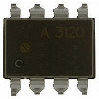
ACPL-312U-300E Avago Technologies US Inc., ACPL-312U-300E Datasheet - Page 13

ACPL-312U-300E
Manufacturer Part Number
ACPL-312U-300E
Description
OPTOCOUPLER IGBT 2.5A 8-SMD GW
Manufacturer
Avago Technologies US Inc.
Series
R²Coupler™r
Datasheet
1.ACPL-312U-500E.pdf
(17 pages)
Specifications of ACPL-312U-300E
Voltage - Isolation
3750Vrms
Number Of Channels
1, Unidirectional
Current - Output / Channel
2.5A
Propagation Delay High - Low @ If
300ns @ 7mA ~ 16mA
Current - Dc Forward (if)
20mA
Input Type
DC
Output Type
Push-Pull, Totem-Pole
Mounting Type
Surface Mount
Package / Case
8-SMD Gull Wing
No. Of Channels
1
Optocoupler Output Type
Gate Drive
Input Current
16mA
Output Voltage
30V
Opto Case Style
SMD
No. Of Pins
8
Output Current
500mA
Output Voltage Max
27V
Isolation Voltage
3.75kV
Forward Current If
20mA
Rohs Compliant
Yes
Lead Free Status / RoHS Status
Contains lead / RoHS non-compliant
Applications Information
Eliminating Negative IGBT Gate Drive ACPL-312U
To keep the IGBT firmly off, the ACPL-312U has a very
low maximum V
realizes this very low V
with 1 : (typical) on resistance in its pull down circuit.
When the ACPL-312U is in the low state, the IGBT gate is
shorted to the emitter by Rg + 1 :. Minimizing Rg and
the lead inductance from the ACPL-312U to the IGBT gate
and emitter (possibly by mounting the ACPL-312U on a
small PC board directly above the IGBT) can eliminate the
need for negative IGBT gate drive in many applications
as shown in Figure 25. Care should be taken with such
a PC board design to avoid routing the IGBT collector or
emitter traces close to the ACPL-312U input as this can
result in unwanted coupling of transient signals into the
ACPL-312U and degrade performance. (If the IGBT drain
must be routed near the ACPL-312U input, then the LED
should be reverse-biased when in the off state, to prevent
the transient signals coupled from the IGBT drain from
turning on the ACPL-312U).
Figure 25. Recommended LED drive and application circuit.
Figure 26. ACPL-312U typical application circuit with negative IGBT gate drive.
13
CONTROL
CONTROL
CMOS
DRIVER
CMOS
DRIVER
INPUT
INPUT
+5 V
+5 V
270 :
270 :
OL
specification of 0.5 V. The ACPL-312U
OL
1
2
3
4
1
2
3
4
by using a DMOS transistor
ACPL-312U
8
7
6
5
0.1 μF
8
7
6
5
0.1 μF
+
–
+
–
Selecting the Gate Resistor (Rg) to Minimize IGBT Switching
Losses.
Step 1: Calculate Rg Minimum from the I
cation. The IGBT and Rg in Figure 26 can be analyzed as
a simple RC circuit with a voltage supplied by the ACPL-
312U.
The V
vative value of VOL at the peak current of 2.5A (see Figure
6). At lower Rg values the voltage supplied by the ACPL-
312U is not an ideal voltage step. This results in lower peak
currents (more margin) than predicted by this analysis.
When negative gate drive is not used VEE in the previous
equation is equal to zero volts.
R
=
R
+
–
V
V
g
g
CC
(15 + 5 − 2.5V)
EE
Rg
V
= 7ohm
≥
CC
= 15 V
= -5 V
Rg
OL
2.5 A
(V
= 18 V
CC
value of 2.5V in the previous equation is a conser-
Q1
Q2
− V
I
OLPEAK
Q1
Q2
EE
− V
OL
)
=
(V
CC
I
− V
OLPEAK
3-PHASE
+ HVDC
- HVDC
EE
AC
3-PHASE
− 2.5V )
+ HVDC
- HVDC
AC
OL
Peak Specifi-


