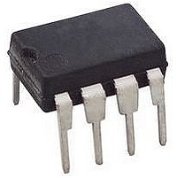
ACPL-312U-000E Avago Technologies US Inc., ACPL-312U-000E Datasheet - Page 14

ACPL-312U-000E
Manufacturer Part Number
ACPL-312U-000E
Description
OPTOCOUPLER IGBT 2.5A 8-DIP
Manufacturer
Avago Technologies US Inc.
Datasheet
1.ACPL-312U-500E.pdf
(17 pages)
Specifications of ACPL-312U-000E
No. Of Channels
1
Optocoupler Output Type
Gate Drive
Input Current
16mA
Output Voltage
30V
Opto Case Style
DIP
No. Of Pins
8
Output Current
500mA
Output Voltage Max
27V
Isolation Voltage
3.75kV
Forward Current If
20mA
Rohs Compliant
Yes
Lead Free Status / RoHS Status
Contains lead / RoHS non-compliant
Available stocks
Company
Part Number
Manufacturer
Quantity
Price
Company:
Part Number:
ACPL-312U-000E
Manufacturer:
ST
Quantity:
4 300
Step 2: Check the ACPL-312U Power Dissipation and Increase
Rg if Necessary.
The ACPL-312U total power dissipation (P
sum of the emitter power (P
P
P
P
For the circuit in Figure 26 with I
Rg = 8 :, Max Duty Cycle = 80%, Qg = 500 nC, f = 20 kHz:
P
P
Step 3: Comparing the calculated power dissipation with the
absolute maximum values for the ACPL-312U:
P
P
Therefore, the power dissipation absolute maximum
rating has not been exceeded for the example.
Figure 27. Energy dissipated in the ACPL-312U for each IGBT switching cycle.
Figure 28. Thermal model.
14
T
T
E
O
E
O
O
T
LC
14
12
10
= 467°C/W
8
6
4
2
0
0
= P
= I
= P
= I
= 16mA . 1.95V . 0.8 = 24.96mW
= 5mA .20V + 5.2PJ .20kHz
= 100mW + 104mW
= 204mW
= 204mW < 370mW (abs. max.)OK
= 24.96mW + 204mW
= 228.96mW < 400mW (abs. max.) OK
T
JE
F
CC
E
O(BIAS)
.V
T
+ P
.(V
LD
F
10
.Duty Cycle
CC
= 442°C/W
O
T C
+ P
- V
T
EE
O (SWITCHING)
CA
T
Rg – GATE RESISTANCE –
A
) + E
= 83°C/W *
T
T
20
DC
JD
SW
E
= 126°C/W
) and the output power (P
(R
G
, Q
F
30
(worst case) = 16 mA,
G
).f
T
T
T
T
*
T
T
T
JD
LC
T
JE
C
DC
CA
LD
T
Qg = 100 nC
Qg = 500 nC
Qg = 1000 nC
V CC = 19 V
V EE = -9 V
:
CA
) is equal to the
40
= LED junction temperature
= detector IC junction temeperature
= case temperature measured at the ce nter of the package bottom
= LED-to-case thermal resistance
= LED-to-detector thermal resistance
= detector-to-case thermal resistance
= case-to-ambient thermal resistance
will depend on the board design and the placement of the part.
50
O
):
Thermal Model
The steady state thermal model for the ACPL-312U is
shown in Figure 28. The thermal resistance values given
in this model can be used to calculate the temperatures
at each node for a given operating condition. As shown
by the model, all heat generated flows through T
raises the case temperature TC accordingly. The value of
T
therefore, determined by the designer. The value of T
83°C/W was obtained from thermal measurements using
a 2.5 x 2.5 inch PC board, with small traces (no ground
plane), a single ACPL-312U soldered into the center of
the board and still air. The absolute maximum power dis-
sipation de-rating specifications assume a T
83°C/W. From the thermal mode in Figure 28 the LED and
detector IC junction temperatures can be expressed as:
Inserting the values for T
gives:
T
T
For example, given P
and T
T
T
T
layout and part placement (T
tion.
JE
JD
JE
JD
JE
CA
T
+ P
T
+P
and T
depends on the conditions of the board design and is,
JE
JD
D
CA
D
= P
= P
. (T
. ( T
= 83°C/W:
JD
= P
= P
= P
= 30 mW.339°C/W + 230 mW .140°C/W + 100°C
= 142°C
= P
= 30 mW.140°C/W + 230 mW.194°C/W + 100°C
= 149°C
E
E
T
DC
=(T
( T
should be limited to 150°C based on the board
LC +
E
E
E
E
T
T
.(256°C/W + T
.(57°C/W + T
.339°C/W + P
.140°C/W + P
|| T
LC +
LC *
LC
T
T
LD +
DC +
LC
|| T
T
T
DC +
. T
DC
LC +
T
T
E
DC
LC
LD
= 30 mW, P
T
T
) + T
LD
DC
CA
LC
D
D
CA
.140°C/W + T
.194°C/W + T
) + T
) + P
CA
CA
and T
) + P
) + T
CA
) + T
CA
CA
D
)
) specific to the applica-
D
.(111°C/W + T
O
)
A
A
.(57°C/W + T
DC
= 230 mW, T
shown in Figure 28
A
A
CA
CA
CA
A
CA
value of
) + T
) + T
= 100°C
which
CA
A
A
=


