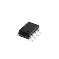
HCPL-7601#300 Avago Technologies US Inc., HCPL-7601#300 Datasheet - Page 10

HCPL-7601#300
Manufacturer Part Number
HCPL-7601#300
Description
OPTOCOUPLER 10MBD 8-SMD GW
Manufacturer
Avago Technologies US Inc.
Datasheet
1.HCPL-7611.pdf
(13 pages)
Specifications of HCPL-7601#300
Package / Case
8-SMD Gull Wing
Voltage - Isolation
3750Vrms
Number Of Channels
1, Unidirectional
Current - Output / Channel
50mA
Data Rate
10MBd
Propagation Delay High - Low @ If
57ns @ 4mA
Current - Dc Forward (if)
20mA
Input Type
DC
Output Type
Open Collector
Mounting Type
Surface Mount, Gull Wing
Isolation Voltage
3750 Vrms
Maximum Continuous Output Current
50 mA
Maximum Fall Time
10 ns
Maximum Forward Diode Current
20 mA
Maximum Rise Time
24 ns
Minimum Forward Diode Voltage
1.2 V
Output Device
Logic Gate Photo IC
Configuration
1 Channel
Maximum Baud Rate
10 MBps
Maximum Forward Diode Voltage
1.85 V
Maximum Reverse Diode Voltage
3 V
Maximum Power Dissipation
250 mW
Maximum Operating Temperature
+ 85 C
Minimum Operating Temperature
- 40 C
Lead Free Status / RoHS Status
Contains lead / RoHS non-compliant
Available stocks
Company
Part Number
Manufacturer
Quantity
Price
Notes:
Figure 1. High level output current vs.
temperature.
Figure 4. Output voltage vs. forward input
current.
10
1. Bypassing of the power supply line is
2. Peaking circuits may produce transient
3. Device considered a two terminal device:
4. The t
required with a 0.1 F ceramic disc
capacitor adjacent to each optocoupler, as
illustrated in Figure 15. Total lead length
between both ends of the capacitor and
the isolator pins should not exceed 10 mm.
input currents up to 50 mA, 50 ns maximum
pulse width, provided average current does
not exceed 20 mA.
pins 1 , 2, 3, and 4 shorted together, and
pins 5, 6, 7, and 8 shorted together.
from the 50% point on the trailing edge of
the input pulse to the 1.5 V point on the
trailing edge of the output pulse.
5.0
4.0
3.0
2.0
1.0
10
15
5
0
0
-60 -40 -20
0
I
F
PLH
– FORWARD INPUT CURRENT – mA
propagation delay is measured
T
A
0.5
– TEMPERATURE – °C
0
1.0
20
R
R
R
L
L
40
L
= 350
= 1 k
= 4 k
V
V
V
CC
O
IN
1.5
60
= 5.5 V
= 0.8 V
= 5.5 V
80 100
2.0
Figure 2. Low level output voltage vs.
temperature.
Figure 5. Input threshold current vs.
temperature.
5. The t
6. t
7. CM
8. CM
from the 50% point on the leading edge of
the input pulse to the 1.5 V point on the
leading edge of the output pulse.
t
units at any given temperature within the
operating condition range.
of the common mode voltage to assure
that the output will remain in a high logic
state (i.e., V
of the common mode voltage to assure
that the output will remain in a low logic
state (i.e., V
0.5
2.5
2.0
1.5
1.0
PSK
PHL
0.6
0.5
0.4
0.3
0.2
0
-60 -40 -20
-60 -40 -20
H
L
is equal to the worst case difference in
and/or t
is the maximum tolerable rate of fall
PHL
is the maximum tolerable rate of rise
propagation delay is measured
I
I
O
O
T
T
OUT
OUT
A
= 16.0 mA
= 13.0 mA
A
PLH
– TEMPERATURE – °C
– TEMPERATURE – °C
> 2.0 V).
< 0.8 V). This specification
that will be seen between
0
0
20
20
V
V
I
40
O
40
CC
O
V
I
= 13.0 mA
F
= 0.6 V
CC
= 2 - 4 mA
= 5.0 V
60
60
= 5.5 V
80 100
80 100
10. AC performance at I
Figure 3. Typical input forward current vs.
input forward voltage.
Figure 6. Low level output current vs.
temperature.
9. In accordance with UL and CSA
10
10 -2
10
10
10
10
assumes that good board layout proce-
dures were followed to reduce the
effective input/output capacitance as
shown in Figure 15.
requirements, each optocoupler is proof
tested by applying an insulation test
voltage 5000 Vrms for one second
(leakage detection current limit,
I
approximately equivalent to the HCPL-
2601/11 at I
purposes.
I-O
55
50
45
40
35
30
-1
-3
-4
-5
-6
-50
0.8
V
5 A).
F
– INPUT FORWARD VOLTAGE – V
V
V
-30
1.0
CC
OL
T
T
A
A
F
= 5 V
= 0.6 V
-10
– TEMPERATURE – °C
= 7.5 mA for comparison
= 85° C
1.2
0
T
A
10
F
= 25° C
I
= 4 mA is
1.4
F
= 2 mA
30
I
F
1.6
= 4 mA
T
50
A
= -40° C
1.8
70
2.0
90


