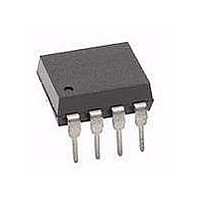
HCPL-3120-060E Avago Technologies US Inc., HCPL-3120-060E Datasheet - Page 21

HCPL-3120-060E
Manufacturer Part Number
HCPL-3120-060E
Description
OPTOCOUPLER 1CH 2.5A VDE 8-DIP
Manufacturer
Avago Technologies US Inc.
Datasheet
1.HCPL-3120-500E.pdf
(24 pages)
Specifications of HCPL-3120-060E
Configuration
1 Channel
Isolation Voltage
3750 Vrms
Output Type
Open Collector
Maximum Propagation Delay Time
500 ns
Maximum Forward Diode Voltage
1.8 V
Minimum Forward Diode Voltage
1.2 V
Maximum Reverse Diode Voltage
5 V
Maximum Forward Diode Current
25 mA
Maximum Power Dissipation
295 mW
Maximum Operating Temperature
+ 100 C
Minimum Operating Temperature
- 40 C
Package / Case
PDIP-8
No. Of Channels
1
Optocoupler Output Type
Gate Drive
Input Current
16mA
Output Voltage
30V
Opto Case Style
DIP
No. Of Pins
8
Propagation Delay Low-high
0.5µs
Rohs Compliant
Yes
Common Mode Ratio
15 KV/uS
Lead Free Status / RoHS Status
Lead free / RoHS Compliant
Lead Free Status / RoHS Status
Lead free / RoHS Compliant, Lead free / RoHS Compliant
Available stocks
Company
Part Number
Manufacturer
Quantity
Price
Company:
Part Number:
HCPL-3120-060E
Manufacturer:
AVAGO
Quantity:
10 000
Part Number:
HCPL-3120-060E
Manufacturer:
AVAGO/安华高
Quantity:
20 000
θ
LED Drive Circuit Considerations for Ultra High CMR Per-
formance. (Discussion applies to HCPL-3120, HCPL-J312,
and HCNW3120)
Without a detector shield, the dominant cause of op-
tocoupler CMR failure is capacitive coupling from the
input side of the optocoupler, through the package, to
the detector IC as shown in Figure 29. The HCPL-3120
improves CMR perform-ance by using a detector IC with
an optically transparent Faraday shield, which diverts the
capacitively coupled current away from the sensitive IC
circuitry. However, this shield does not eliminate the ca-
pacitive coupling between the LED and optocoupler pins
5-8 as shown in Figure 30. This capacitive coupling causes
Figure 28. Thermal model.
Figure 29. Optocoupler input to output capacitance model for unshielded
optocouplers.
21
LC
1
2
3
4
= 467 °C/W
C
C
LEDP
LEDN
HCPL-3120 fig 29
T
JE
θ
LD
= 442 °C/W
T
C
θ
CA
T
A
= 83 °C/W*
θ
T
DC
JD
= 126 °C/W
8
7
6
5
HCPL-3120 fig 28
T
T
T
q
q
q
q
*q
DC
LD
CA
JD
LC
JE
C
CA
= LED junction temperature
= detector IC junction temperature
= case temperature measured at the center of the package bottom
= LED-to-case thermal resistance
= LED-to-detector thermal resistance
= detector-to-case thermal resistance
= case-to-ambient thermal resistance
*θ
θ
θ
θ
θ
T
T
T
LC
LD
DC
CA
CA
will depend on the board design and the placement of the part.
JE
JD
C
= CASE TEMPERATURE MEASURED AT THE
= LED JUNCTION TEMPERATURE
= DETECTOR IC JUNCTION TEMPERATURE
= LED-TO-CASE THERMAL RESISTANCE
= LED-TO-DETECTOR THERMAL RESISTANCE
= DETECTOR-TO-CASE THERMAL RESISTANCE
= CASE-TO-AMBIENT THERMAL RESISTANCE
WILL DEPEND ON THE BOARD DESIGN AND
THE PLACEMENT OF THE PART.
CENTER OF THE PACKAGE BOTTOM
perturbations in the LED current during common mode
transients and becomes the major source of CMR failures
for a shielded optocoupler. The main design objective of
a high CMR LED drive circuit becomes keeping the LED
in the proper state (on or off ) during common mode
transients. For example, the recommended application
circuit (Figure 25), can achieve 25 kV/µs CMR while mini-
mizing component complexity.
Techniques to keep the LED in the proper state are
discussed in the next two sections.
Figure 30. Optocoupler input to output capacitance model for shielded
optocouplers.
1
2
3
4
C
C
LEDP
LEDN
HCPL-3120 fig 30
C
SHIELD
LEDO1
C
LEDO2
8
7
6
5


