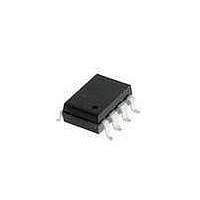
HCPL-T250#300 Avago Technologies US Inc., HCPL-T250#300 Datasheet - Page 7

HCPL-T250#300
Manufacturer Part Number
HCPL-T250#300
Description
OPTOCOUPLER DRIVER 1.5A 8-SMD GW
Manufacturer
Avago Technologies US Inc.
Datasheet
1.HCPL-T250-500E.pdf
(7 pages)
Specifications of HCPL-T250#300
Output Type
Push-Pull, Totem-Pole
Package / Case
8-SMD Gull Wing
Voltage - Isolation
3750Vrms
Number Of Channels
1, Unidirectional
Current - Output / Channel
1.5A
Propagation Delay High - Low @ If
270ns @ 7mA ~ 16mA
Current - Dc Forward (if)
25mA
Input Type
DC
Mounting Type
Surface Mount, Gull Wing
Configuration
1 Channel
Isolation Voltage
3750 Vrms
Maximum Propagation Delay Time
500 ns
Maximum Forward Diode Voltage
1.8 V
Maximum Reverse Diode Voltage
5 V
Maximum Forward Diode Current
16 mA
Maximum Power Dissipation
250 mW
Maximum Operating Temperature
+ 85 C
Minimum Operating Temperature
- 20 C
Lead Free Status / RoHS Status
Contains lead / RoHS non-compliant
Available stocks
Company
Part Number
Manufacturer
Quantity
Price
For product information and a complete list of distributors, please go to our website:
Avago, Avago Technologies, and the A logo are trademarks of Avago Technologies Limited in the United States and other countries.
Data subject to change. Copyright © 2007 Avago Technologies Limited. All rights reserved. Obsoletes 5989-2144EN
AV02-0166EN - October 16, 2007
7
Switching Specifications (AC)
Over recommended operating conditions (T
V
*All typical values at T
Notes:
4. The difference between t
5. Common mode transient immunity in the high state is the maximum tolerable dV
6. Common mode transient immunity in a low state is the maximum tolerable dV
CC
Parameter
Propagation Delay
Time to High
Output Level
Propagation Delay
Time to Low
Output Level
Output Rise Time
Output Fall Time
Pulse Width
Distortion
Propagation
Delay Difference
Between Any
Two Parts
Output High
Level Common
Mode Transient
Immunity
Output Low
Level Common
Mode Transient
Immunity
output will remain in the high state (i.e., V
put will remain in a low state (i.e., V
= 15 to 30 V, V
A
EE
= 25°C and V
= Ground) unless otherwise specified.
Symbol
(t
|CM
|CM
PHL
PWD
t
T
PDD
t
PHL
PLH
PHL
PLH
t
t
R
F
and t
H
L
)
‑
|
|
CC
(Compared with HCPL‑3120)
PLH
O
kV/µs
kV/µs
Units
‑ V
< 1.0 V).
µs
µs
µs
µs
µs
µs
between any two HCPL‑3120 parts under the same test condition.
EE
= 30 V, unless otherwise noted.
O
> 15.0 V).
‑0.35
Min.
0.1
0.1
25
25
(-40°C ~ 100°C)
A
HCPL-3120
= ‑40 to 100°C, I
Typ.*
0.27
0.3
0.1
0.1
35
35
Max.
0.35
0.5
0.5
0.3
www.avagotech.com
N.A.
N.A.
N.A.
F(ON)
Min.
5
5
CM
(-20°C ~ 85°C)
= 7 to 16 mA, V
HCPL-T250
/dt of the common mode pulse, V
CM
Typ.*
0.27
0.3
/dt of the common mode pulse, V
Max.
N.A.
N.A.
0.5
0.5
F(OFF)
V
HCPL
‑3120
HCPL
‑T250
V
HCPL
‑3120
HCPL
‑T250
T
T
A
A
CC
F
= 0 V
= 25°C
= 25°C
Rg = 10 Ω
Cg = 10 nF,
f = 10 kHz,
Duty Cycle = 50%
= 30 V
= ‑3.6 to 0.8 V,
Conditions
CM
Test
I
V
I
V
V
V
F
F
, to assure that the out‑
CM
CM
CM
CM
CM
= 10 mA
= 10 mA
, to assure that the
= 1500 V
= 600 V
= 1500 V
= 600 V
Note
4
5
5


