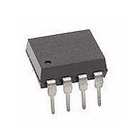
HCNW138 Avago Technologies US Inc., HCNW138 Datasheet

HCNW138
Specifications of HCNW138
Available stocks
Related parts for HCNW138
HCNW138 Summary of contents
Page 1
... LSTTL or other low power appli ca tions. A 400% mini- mum current transfer ratio is guaranteed over 0 to 70°C operating range for only 0 LED current. The 6N138, HCPL-0700, and HCNW138 are designed for use mainly in TTL applications. Current Transfer Ratio (CTR) is 300% minimum over 0 to 70°C for an LED current of 1 TTL Unit load ). A 300% minimum CTR enables operation with 1 TTL Load using a 2.2 kΩ ...
Page 2
... Note: 1. Technical data are on separate Avago publications. 2 lead profile is designed to be compatible with standard surface mount processes. The HCNW139 and HCNW138 are packaged in a widebody encapsulation that provides creep age and clearance dimensions suitable for safety approval by regulatory agencies worldwide. Widebody ...
Page 3
... SO-8 HCPL-0700 -500E #500 SO-8 HCPL-0701 -060E #060 SO-8 -560E #560 SO-8 HCNW138 -000E no option 400 mil HCNW139 -300E #300 Widebody -500E #500 DIP-8 To order, choose a part number from the part number column and combine with the desired option from the option column to form an order entr y ...
Page 4
Package Outline Drawings 8-Pin DIP Package (6N139/6N138)** 9.65 ± 0.25 (0.380 ± 0.010 TYPE NUMBER A XXXXZ YYWW 1.19 (0.047) MAX. 3.56 ± 0.13 (0.140 ± 0.005) 1.080 ± 0.320 (0.043 ± 0.013) **JEDEC ...
Page 5
... TOTAL PACKAGE LENGTH (INCLUSIVE OF MOLD FLASH) 5.207 ± 0.254 (0.205 ± 0.010) DIMENSIONS IN MILLIMETERS (INCHES). LEAD COPLANARITY = 0.10 mm (0.004 INCHES) MAX. NOTE: FLOATING LEAD PROTRUSION IS 0. mils) MAX. 8-Pin Widebody DIP Package (HCNW139/HCNW138) 11.23 ± 0.15 (0.442 ± 0.006 HCNWXXXX ...
Page 6
... Widebody DIP Package with Gull Wing Surface Mount Option 300 (HCNW139/HCNW138) 11.23 ± 0.15 (0.442 ± 0.006 1.80 ± 0.15 (0.071 ± 0.006) 2.54 (0.100) BSC DIMENSIONS IN MILLIMETERS (INCHES). LEAD COPLANARITY = 0.10 mm (0.004 INCHES). NOTE: FLOATING LEAD PROTRUSION IS 0.25 mm (10 mils) MAX. ...
Page 7
Recommended Pb-Free IR Profile * 260 +0/-5 ° 217 ° RAMP-UP 3 °C/SEC. MAX. 150 - 200 °C T smax T smin t s PREHEAT 60 to 180 SEC °C to PEAK TIME ...
Page 8
... IEC/EN/DIN EN 60747-5-2 Insulation Related Characteristics (HCNW139 and HCNW138) Description Installation Classification per DIN VDE 0110/1.89, Table 1 for rated mains voltage ≤600 V rms for rated mains voltage ≤1000 V rms Climatic Classification Pollution Degree (DIN VDE 0110/1.89) Maximum Working Insulation Voltage Input to Output Test Voltage, Method b* ...
Page 9
... Output Current (Pin 6) Emitter Base Reverse Voltage (Pin 5-7) Supply Voltage and Output Voltage (6N139, HCPL-0701, HCNW139) Supply Voltage and Output Voltage (6N138, HCPL-0700, HCNW138) Output Power Dissipation Total Power Dissipation Lead Solder Temperature (for Through Hole Devices) Reflow Temperature Profile (for SOIC-8 and Option #300) *JEDEC Registered Data for 6N139 and 6N138 ...
Page 10
... HCNW138 Logic High I 6N138/139 CCH Supply Current HCPL-0701/ 0700 HCNW139 HCNW138 Input Forward V 6N138 F Voltage 6N139 HCPL-0701 HCPL-0700 HCNW139 HCNW138 Input Reverse BVR HCNW139 Breakdown Voltage HCNW138 Temperature ∆V F Coefficient of ∆T A Forward Voltage Input C IN Capacitance HCNW139 HCNW138 *JEDEC Registered Data for 6N139 and 6N138. ...
Page 11
... HCNW139 6N138 HCPL-0700 HCNW138 Propagation t 6N139 PLH Delay Time HCPL-0701 to Logic High HCNW139 at Output 6N139 HCPL-0701 HCNW139 6N138 HCPL-0700 HCNW138 Common Mode | Transient Immunity at Logic High Output Common Mode | Transient Immunity at Logic Low Output *JEDEC Registered Data for 6N139 and 6N138. ...
Page 12
... Package Characteristics Parameter Input-Output Momentary Withstand Voltage† Option 020 HCNW139 HCNW138 Resistance (Input-Output) Capacitance (Input-Output) **All typicals 25°C, unless otherwise noted. A †The Input-Output Momentary Withstand Voltage is a dielectric voltage rating that should not be interpreted as an input-output continuous voltage rating. For the continuous voltage rating refer to the IEC/EN/DIN EN 60747-5-2 Insulation Characteristics Table (if applicable), your equipment level safety specification or Avago Application Note 1074 entitled “ ...
Page 13
25° 1.0 2.0 V – OUTPUT VOLTAGE – Figure 1. 6N138/6N139 DC transfer character- istics 6N1390 fig ...
Page 14
0 0.3 0.2 0 – FORWARD CURRENT F Figure 10. Logic low supply current vs. forward ...


