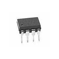
HCPL-3140-300E Avago Technologies US Inc., HCPL-3140-300E Datasheet - Page 7

HCPL-3140-300E
Manufacturer Part Number
HCPL-3140-300E
Description
OPTOCOUPLER 1CH 0.4A 8-SMD GW
Manufacturer
Avago Technologies US Inc.
Datasheet
1.HCPL-3140-000E.pdf
(16 pages)
Specifications of HCPL-3140-300E
Voltage - Isolation
3750Vrms
Number Of Channels
1, Unidirectional
Current - Output / Channel
600mA
Propagation Delay High - Low @ If
300ns @ 8mA
Current - Dc Forward (if)
25mA
Input Type
DC
Output Type
Push-Pull, Totem-Pole
Mounting Type
Surface Mount, Gull Wing
Package / Case
8-SMD Gull Wing
No. Of Channels
1
Optocoupler Output Type
Gate Drive
Input Current
12mA
Output Voltage
30V
Opto Case Style
SMD
No. Of Pins
8
Peak Reflow Compatible (260 C)
Yes
Isolation Voltage
3.75kV
Lead Free Status / RoHS Status
Lead free / RoHS Compliant
Available stocks
Company
Part Number
Manufacturer
Quantity
Price
Company:
Part Number:
HCPL-3140-300E
Manufacturer:
AVAGO
Quantity:
26 000
Part Number:
HCPL-3140-300E
Manufacturer:
AVAGO/安华高
Quantity:
20 000
Switching Specifications (AC)
Over recommended operating conditions unless otherwise specified.
Notes:
1. Derate linearly above 70 C free air temperature at a rate of 0.3 mA/ C.
2. Maximum pulse width = 10 s, maximum duty cycle = 0.2%. This value is intended to allow for component tolerances for designs with I
3. Derate linearly above 85 C, free air temperature at the rate of 4.0 mW/ C.
4. Input power dissipation does not require derating.
5. Maximum pulse width = 50 s, maximum duty cycle = 0.5%.
6. In this test, V
7. Maximum pulse width = 1 ms, maximum duty cycle = 20%.
8. In accordance with UL 1577, each optocoupler is proof tested by applying an insulation test voltage 4500 V
9. Device considered a two-terminal device: pins on input side shorted together and pins on output side shorted together.
10. PDD is the difference between t
11. Common mode transient immunity in the high state is the maximum tolerable |dVcm/dt| of the common mode pulse V
12. Common mode transient immunity in a low state is the maximum tolerable |dV
13. This load condition approximates the gate load of a 1200 V/25 A IGBT.
14. The power supply current increases when operating frequency and Qg of the driven IGBT increases.
7
Package Characteristics
Parameter
Propagation Delay Time to
High Output Level
Propagation Delay Time to
Low Output Level
Propagation Delay
Difference Between Any
Two Parts or Channels
Rise Time
Fall Time
Output High Level Common
Mode Transient Immunity
Output Low Level Common
Mode Transient Immunity
Parameter
Input-Output Momentary
Withstand Voltage
Input-Output Resistance
Input-Output Capacitance
minimum = 0.4 A. See Application section for additional details on limiting I
current limit I
60747-5-2 Insulation Characteristics Table, if applicable.
will remain in the high state (i.e. Vo > 6.0 V).
will remain in a low state (i.e. Vo < 1.0 V).
OH
I-O
is measured with a DC load current. When driving capacitive load V
5 A). This test is performed before 100% production test for partial discharge (method B) shown in the IEC/EN/DIN EN
PHL
and t
Symbol
V
R
C
Symbol
t
t
PDD
t
t
|CM
|CM
PLH
PHL
R
F
ISO
I-O
I-O
PLH
H
L
between any two parts or channels under the same test conditions.
|
|
Min.
0.1
0.1
-0.5
25
25
Min.
3750
Typ.
0.2
0.3
50
50
35
35
Typ.
10
0.6
12
OL
peak.
CM
Max.
0.7
0.7
0.5
Max.
/dt| of the common mode pulse, V
OH
will approach V
Units
V
pF
Units
ns
ns
kV/ s
kV/ s
s
s
s
rms
CC
Test
Conditions
Rg = 47 ,
Cg = 3 nF,
f = 10 kHz,
Duty Cycle =
50%,
I
V
T
V
Test
Conditions
T
RH<50% for
V
Freq=1 MHz
F =
as I
CC
A
CM
A
I-O
=25 C,
= 25 C,
8 mA,
rms
= 30 V
=500 V
OH
= 1 kV
approaches zero amps.
for 1 second (leakage detection
CM
CM
, to assure that the output
to assure that the output
Fig.
Fig.
10,11,
12,13,
14,17
18
18
O
Note
8,9
9
peak
Note
14
10
11
12


