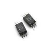
ACPL-W60L-560E Avago Technologies US Inc., ACPL-W60L-560E Datasheet - Page 10

ACPL-W60L-560E
Manufacturer Part Number
ACPL-W60L-560E
Description
OPTOCOUPLER 15MBD 3.3V VDE 6SOIC
Manufacturer
Avago Technologies US Inc.
Specifications of ACPL-W60L-560E
Package / Case
6-SOP
Voltage - Isolation
3750Vrms
Number Of Channels
1, Unidirectional
Current - Output / Channel
50mA
Data Rate
15MBd
Propagation Delay High - Low @ If
75ns @ 7.5mA
Current - Dc Forward (if)
20mA
Input Type
DC
Output Type
Open Collector
Mounting Type
Surface Mount
Isolation Voltage
3750 Vrms
Maximum Continuous Output Current
50 mA
Maximum Fall Time
20 ns
Maximum Forward Diode Current
20 mA
Maximum Rise Time
45 ns
Minimum Forward Diode Voltage
1.4 V
Output Device
Logic Gate Photo IC
Configuration
1 Channel
Maximum Baud Rate
15 MBps
Maximum Forward Diode Voltage
1.75 V
Maximum Reverse Diode Voltage
5 V
Maximum Power Dissipation
85 mW
Maximum Operating Temperature
+ 85 C
Minimum Operating Temperature
- 40 C
Number Of Elements
1
Forward Voltage
1.75V
Forward Current
20mA
Output Current
50mA
Operating Temp Range
-40C to 85C
Power Dissipation
85mW
Propagation Delay Time
90ns
Pin Count
6
Mounting
Surface Mount
Reverse Breakdown Voltage
5V
Operating Temperature Classification
Industrial
Lead Free Status / RoHS Status
Lead free / RoHS Compliant
Lead Free Status / RoHS Status
Lead free / RoHS Compliant, Lead free / RoHS Compliant
Package Characteristics
All Typicals at T
Parameter
Input-Output
Insulation
Input-Output
Momentary
Withstand
Voltage*
Input-Output
Resistance
Input-Output
Capacitance
Input-Input
Insulation
Leakage
Current
Resistance
(Input-Input)
Capacitance
(Input-Input)
*The Input-Output Momentary Withstand Voltage is a dielectric voltage rating that should not be interpreted as an input-output continuous volt-
age rating. For the continuous voltage rating refer to the IEC/EN/DIN EN 60747-5-2 Insulation Characteristics Table (if applicable), your equipment
level safety specification or Avago Application Note 1074 entitled "Optocoupler Input-Output Endurance Voltage."
Notes:
1. Each channel.
2
3. Peaking circuits may produce transient input currents up to 50 mA, 50 ns maximum pulse width, provided average current does not exceed
4. Derate linearly above +80˚C free-air temperature at a rate of 2.7 mW/˚C.
5. Bypassing of the power supply line is required, with a 0.1 μF ceramic disc capacitor adjacent to each optocoupler as illustrated in Figure 11.
6. The t
7. The t
8. t
9. See test circuit for measurement details.
10. CM
11. CM
12. For sinusoidal voltages, (|dV
13. Single channel device is considered a two-terminal part when pins 1, 2, 3 are shorted together, and pins 4, 5, 6 shorted together separately.
14. In accordance with UL 1577, each optocoupler is proof tested by applying an insulation test voltage ≥ 6000 V rms for one second (leakage
15. Measured between the LED anode and cathode shorted together and pins 5 through 8 shorted together. For dual channel products only.
16. Measured between pins 1 and 2 shorted together, and pins 3 and 4 shorted together. For dual channel products only.
10
Peaking circuits may produce transient input currents up to 50 mA, 50 ns maximum pulse width, provided average current does not exceed
20 mA.
15 mA.
Total lead length between both ends of the capacitor and the isolator pins should not exceed 20 mm.
of the output pulse.
of the output pulse.
ditions.
(i.e., V
(i.e., V
Dual channel device is considered a two-terminal part when pins 1, 2, 3, 4 are shorted together, and pins 5, 6, 7, 8 are shorted together
separately.
detection current limit, I
EN/DIN EN 60747-5-2 Insulation Characteristics Table, if applicable.
PSK
H
L
is equal to the worst case difference in t
is the maximum tolerable rate of fall of the common mode voltage to assure that the output will remain in a low logic state
PLH
PHL
is the maximum tolerable rate of rise on the common mode voltage to assure that the output will remain in a high logic state
o
o
> 2.0 V).
< 0.8 V).
propagation delay is measured from the 3.75 mA point on the falling edge of the input pulse to the 1.5 V point on the rising edge
propagation delay is measured from the 3.75 mA point on the rising edge of the input pulse to the 1.5 V point on the falling edge
A
Sym.
I
V
R
C
I
R
C
= 25˚C.
I-O
I-I
I-O
I-I
ISO
I-O
I-I
*
I-O
Dual Channel
Package
Single
Single,
Dual Channel
Single,
Single,
Dual Channel
Dual Channel
Dual Channel
Dual Channel
≤ 5 μA). This test is performed before the 100% production test for partial discharge (Method b) shown in the IEC/
CM
| / dt)
max
= πf
PHL
CM
V
and/or t
CM
Min.
5000
(p-p).
PLH
that will be seen between units at any given temperature and specified test con-
Typ.
10
0.5
0.005
10
0.25
12
11
Max
1
μA
V rms
Ω
pF
μA
Ω
pG
nits
Test Conditions
45% RH, t = 5 s,
V
RH ≤ 50%, t = 1 min,
T
V
f = 1 MHz, T
RH ≤ 45%, t = 5 s,
V
f = 1 MHz
A
I-O
I-O
I-I
= 25˚C
= 500 V
= 3 kV DC, T
=500 V dc
A
= 25˚C
A
= 25˚C
Fig.
13, 14
13, 14
1, 13, 15
1, 13, 15
16
16
16
ote


