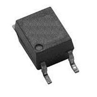
HCPL-M456-560E Avago Technologies US Inc., HCPL-M456-560E Datasheet - Page 8

HCPL-M456-560E
Manufacturer Part Number
HCPL-M456-560E
Description
OPTOCOUPLER IPM 1MBD IEC SO-5
Manufacturer
Avago Technologies US Inc.
Datasheet
1.HCPL-M456500.pdf
(13 pages)
Specifications of HCPL-M456-560E
Voltage - Isolation
3750Vrms
Number Of Channels
1, Unidirectional
Current - Output / Channel
15mA
Propagation Delay High - Low @ If
200ns @ 10mA
Current - Dc Forward (if)
25mA
Input Type
DC
Output Type
Open Collector
Mounting Type
Surface Mount
Package / Case
5-SOP
No. Of Channels
1
Optocoupler Output Type
Gate Drive
Input Current
20mA
Output Voltage
30V
Opto Case Style
SOIC
No. Of Pins
5
Ctr Max
90%
Isolation Voltage
3.75kV
Lead Free Status / RoHS Status
Lead free / RoHS Compliant
8
IPM Dead Time and Propagation Delay Specifications
The HCPL-M456 includes a Propagation Delay Differ-
ence specification intended to help designers mini-
mize “dead time” in their power inverter designs. Dead
time is the time period during which both the high
and low side power transistors (Q1 and Q in Figure
) are off. Any overlap in Q1 and Q conduction will
result in large currents flowing through the power
devices between the high and low voltage motor rails.
To minimize dead time the designer must consider the
propagation delay characteristics of the optocoupler
as well as the characteristics of the IPM IGBT gate drive
circuit. Considering only the delay characteristics of the
optocoupler (the characteristics of the IPM IGBT gate
drive circuit can be analyzed in the same way) it is im-
portant to know the minimum and maximum turn-on
(t
preferably over the desired operating temperature range.
The limiting case of zero dead time occurs when the
input to Q1 turns off at the same time that the input to
Q turns on. This case determines the minimum delay
between LED1 turn-off and LED turn-on, which is re-
lated to the worst case optocoupler propagation delay
waveforms, as shown in Figure 3. A minimum dead
time of zero is achieved in Figure 3 when the signal to
Figure 2. Typical Transfer Characteristics.
PHL
10
8
6
4
2
0
) and turn-off (t
0
I
F
– FORWARD CURRENT – mA
5
HCPL-M456 fig 2
10
PLH
) propagation delay specifications,
V
O
= 0.6 V
100 °C
25 °C
-40 °C
15
20
Figure 3. Normalized Output Current vs. Temperature.
1.05
1.00
0.95
0.90
0.85
0.80
-40
-20
T
A
– TEMPERATURE – °C
0
HCPL-M456 fig 3
20
turn on LED is delayed by (t
LED1 turn off. Note that the propagation delays used to
calculate PDD are taken at equal temperatures since the
optocouplers under consideration are typically mounted
in close proximity to each other. (Specifically, t
and t
the t
ture range, specified in the data sheet.) This delay is the
maximum value for the propagation delay difference
specification which is specified at 370 ns for the HCPL-M456
over an operating temperature range of -40°C to 100°C.
Delaying the LED signal by the maximum propagation
delay difference ensures that the minimum dead time is
zero, but it does not tell a designer what the maximum
dead time will be. The maximum dead time occurs in the
highly unlikely case where one optocoupler with the fast-
est t
inverter leg. The maximum dead time in this case becomes
the sum of the spread in the t
delays as shown in Figure 4. The maximum dead time is
also equivalent to the difference between the maximum
and minimum propagation delay difference specifica-
tions. The maximum dead time (due to the optocouplers)
for the HCPL-M456 is 50 ns (= 370 ns - (-150 ns)) over an
operating temperature range of -40°C to 100°C.
40
I
V
PLH
F
PLH max
O
PHL min
= 10 mA
60
= 0.6 V
and another with the slowest t
80
and t
in the previous equation are not the same as
100
PHL min
Figure 4. High Level Output Current vs. Temperature.
, over the full operating tempera-
2.0
1.5
1.0
0.5
0
-40
V
V
-20
F
CC
PLH max
= 0.8 V
T
PLH
A
= V
4.5 V
30 V
– TEMPERATURE – °C
0
HCPL-M456 fig 4
O
and t
= 4.5 V OR 30 V
- t
20
PHL
PHL min
PHL
are in the same
40
propagation
) from the
60
80
PLH max
100


