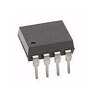
6N137#500 Avago Technologies US Inc., 6N137#500 Datasheet - Page 17

6N137#500
Manufacturer Part Number
6N137#500
Description
OPTOCOUPLER 1CH 10MBD 8-SMD
Manufacturer
Avago Technologies US Inc.
Datasheet
1.HCPL-0600-500E.pdf
(22 pages)
Specifications of 6N137#500
Input Type
DC
Package / Case
8-SMD
Voltage - Isolation
3750Vrms
Number Of Channels
1, Unidirectional
Current - Output / Channel
50mA
Data Rate
10MBd
Propagation Delay High - Low @ If
50ns @ 7.5mA
Current - Dc Forward (if)
20mA
Output Type
Open Collector
Mounting Type
Surface Mount
Isolation Voltage
3750 Vrms
Maximum Continuous Output Current
50 mA
Maximum Fall Time
10 ns
Maximum Forward Diode Current
20 mA
Maximum Rise Time
24 ns
Minimum Forward Diode Voltage
1.4 V
Output Device
Logic Gate Photo IC
Configuration
1 Channel
Maximum Baud Rate
10 MBps
Maximum Forward Diode Voltage
1.75 V
Maximum Reverse Diode Voltage
5 V
Maximum Input Diode Current
20 mA
Maximum Power Dissipation
85 mW
Maximum Operating Temperature
+ 85 C
Minimum Operating Temperature
- 40 C
Lead Free Status / RoHS Status
Contains lead / RoHS non-compliant
Available stocks
Company
Part Number
Manufacturer
Quantity
Price
PULSE GEN.
t = t = 5 ns
MONITORING
f
Z
O
Figure 8. Test circuit for t
Figure 9. Typical propagation delay vs. tem-
perature.
Figure 11. Typical pulse width distortion vs.
temperature.
17
= 50 Ω
r
INPUT
NODE
100
80
60
40
20
-10
30
20
10
0
40
-60
0
-60
t
V
I
PHL
F
CC
R
-40
I
= 7.5 mA
F
-40
M
t
= 5.0 V
, R
PLH
T
A
R
T
-20
R
L
A
L
-20
– TEMPERATURE – °C
L
= 350 Ω
, R
= 350Ω
- TEMPERATURE -
= 4 kΩ
1
2
3
4
1 KΩ
4 KΩ
L
0
SINGLE CHANNEL
t
0
= 350 Ω
PLH
PHL
20
R
20
L
, R
and t
t
PLH
= 1 kΩ
40
L
40
= 1 KΩ
PLH
, R
V
I
F
60
.
CC
L
= 7.5 mA
60
GND
V
= 4 KΩ
CC
= 5.0 V
o
C
80
80
8
7
6
5
OUTPUT
100
100
INPUT
V
I
*C
F
O
0.1μF
BYPASS
L
Figure 10. Typical propagation delay vs. pulse
input current.
Figure 12. Typical rise and fall time vs. tempera-
ture.
IS APPROXIMATELY 15 pF WHICH INCLUDES
PROBE AND STRAY WIRING CAPACITANCE.
*C
105
300
290
L
60
40
20
90
75
60
45
30
+5 V
0
-60
t
5
PHL
t
R
I
V
I
PHL
F
F
V
T
L
CC
-40
CC
A
– PULSE INPUT CURRENT – mA
= 7.5 mA
OUTPUT V
MONITORING
NODE
= 25°C
T
, R
= 5.0 V
= 5.0 V
7
A
-20
t
L
– TEMPERATURE – °C
PLH
= 350 Ω
R
R
R
R
L
L
1 KΩ
4 KΩ
L
L
0
, R
= 1 kΩ
= 350 Ω
= 350 Ω, 1 kΩ, 4 kΩ
9
= 4 kΩ
O
L
20
= 350 Ω
t
t
MONITORING
t
PLH
PLH
PLH
11
40
PULSE GEN.
t = t = 5 ns
f
, R
Z
, R
O
INPUT
NODE
L
L
60
= 50 Ω
r
= 1 KΩ
= 4 KΩ
13
t
t
RISE
FALL
80
R
I
F
M
1.5 V
100
I
I
F
F
15
= 7.50 mA
= 3.75 mA
1
2
3
4
DUAL CHANNEL
GND
V
CC
7
8
6
5
0.1μF
BYPASS
+5 V
R
C
L
L
*
OUTPUT V
MONITORING
NODE
O


