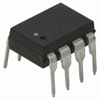
6N138-000E Avago Technologies US Inc., 6N138-000E Datasheet

6N138-000E
Specifications of 6N138-000E
Available stocks
Related parts for 6N138-000E
6N138-000E Summary of contents
Page 1
... CMOS, LSTTL or other low power applications. A 400% minimum current transfer ratio is guaranteed over operating range for only 0 LED current. The 6N138, HCPL-0700, and HCNW138 are designed for use mainly in TTL applications. Current Transfer Ratio (CTR) is 300% minimum over for an LED current of 1 TTL Unit load ). A 300% minimum CTR enables operation with 1 TTL Load using a 2 ...
Page 2
... Single Channel Channel Channel Package Package Package HCPL- HCPL- [1] 6N139 2731 0701 [1] 6N138 2730 0700 [1] [1] HCPL-4701 4731 070A Note: 1. Technical data are on separate Avago publications. 2 The lead profile is designed to be compatible with standard surface mount processes. The HCNW139 and HCNW138 ...
Page 3
... To order, choose a part number from the part number column and combine with the desired option from the option column to form an order entry. Example 1: 6N138-560E to order product of 300 mil DIP Gull Wing Surface Mount package in Tape and Reel packaging with IEC/EN/DIN EN 60747-5-2 Safety Approval and RoHS compliant. Example 2: HCPL-0700 to order product of 300 mil DIP package in Tube packaging and non RoHS compliant ...
Page 4
... TYPE NUMBER A XXXXZ YYWW 1.19 (0.047) MAX. 3.56 ± 0.13 (0.140 ± 0.005) 1.080 ± 0.320 (0.043 ± 0.013) **JEDEC Registered Data. 8-Pin DIP Package with Gull Wing Surface Mount Option 300 (6N139/6N138) 9.65 ± 0.25 (0.380 ± 0.010 1.19 (0.047) MAX. ...
Page 5
Small Outline SO-8 Package (HCPL-0701/HCPL-0700 3.937 ± 0.127 (0.155 ± 0.005 PIN ONE 0.406 ± 0.076 (0.016 ± 0.003) * 5.080 ± 0.127 (0.200 ± 0.005) 3.175 ± 0.127 (0.125 ± 0.005) * TOTAL PACKAGE LENGTH ...
Page 6
Widebody DIP Package with Gull Wing Surface Mount Option 300 (HCNW139/HCNW138) 11.15 ± 0.15 (0.442 ± 0.006 1.78 ± 0.15 (0.070 ± 0.006) 2.54 (0.100) BSC DIMENSIONS IN MILLIMETERS (INCHES). LEAD COPLANARITY = ...
Page 7
Recommended Pb-Free IR Profile 260 +0/-5 ° 217 ° RAMP-UP 3 °C/SEC. MAX. 150 - 200 °C T smax T smin t s PREHEAT 60 to 180 SEC °C to PEAK TIME NOTES: ...
Page 8
IEC/EN/DIN EN 60747-5-2 Insulation Related Characteristics (HCNW139 and HCNW138) Description Installation Classification per DIN VDE 0110/1.89, Table 1 for rated mains voltage 600 V rms for rated mains voltage 1000 V rms Climatic Classification Pollution Degree (DIN VDE 0110/1.89) Maximum ...
Page 9
... Output Power Dissipation Total Power Dissipation Lead Solder Temperature (for Through Hole Devices) Reflow Temperature Profile (for SOIC-8 and Option #300) *JEDEC Registered Data for 6N139 and 6N138. ** JEDEC Registration. Recommended Operating Conditions Parameter Power Supply Voltage Forward Input Current (ON) ...
Page 10
... Breakdown HCNW139 Voltage HCNW138 Temperature V F Coefficient Forward Voltage Input C IN Capacitance HCNW139 HCNW138 *JEDEC Registered Data for 6N139 and 6N138. **All typical values and unless otherwise noted mA 0.8 V, unless otherwise specified. F(ON) F(OFF) Min. Typ.** Max. Units 400* 2000 5000 % ...
Page 11
... HCPL-0701 HCNW139 6N138 HCPL-0700 HCNW138 Common Mode | Transient Immunity at Logic High Output Common Mode | Transient Immunity at Logic Low Output *JEDEC Registered Data for 6N139 and 6N138. **All typical values and unless otherwise noted C unless otherwise specified Min. Typ.** Max 25* 30 0.2 ...
Page 12
Package Characteristics Parameter Input-Output Momentary Withstand Voltage† Option 020 HCNW139 HCNW138 Resistance (Input-Output) Capacitance (Input-Output) **All typicals unless otherwise noted. A †The Input-Output Momentary Withstand Voltage is a dielectric voltage rating that should not be ...
Page 13
... T – TEMPERATURE – °C A Figure 8. Forward voltage vs. temperature. 100 85° 1 70° 25° 0 0° -40° 0.01 0.01 0 – INPUT DIODE FORWARD CURRENT – Figure 3. 6N138/6N139 output current vs. input diode forward current µs t PLH PHL 0 -60 -40 - 100 – TEMPERATURE – °C A Figure 6 ...
Page 14
0 0.3 0.2 0 – FORWARD CURRENT F Figure 10. Logic low supply current vs. ...
Page 15
V 90% 90 10% 10 SWITCH SWITCH AT ...
Page 16
For product information and a complete list of distributors, please go to our website: Avago, Avago Technologies, and the A logo are trademarks of Avago Technologies Limited in the United States and other countries. Data subject to change. Copyright © ...


