VO2630 Vishay, VO2630 Datasheet - Page 5
VO2630
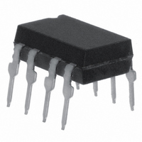
Manufacturer Part Number
VO2630
Description
OPTOCPLR 10MBD 2CH 100V/US 8DIP
Manufacturer
Vishay
Specifications of VO2630
No. Of Channels
2
Input Current
10mA
Output Voltage
7V
Opto Case Style
DIP
No. Of Pins
8
Isolation Voltage
5.3kV
Voltage - Isolation
5300Vrms
Number Of Channels
2, Unidirectional
Current - Output / Channel
50mA
Data Rate
10MBd
Propagation Delay High - Low @ If
50ns @ 7.5mA
Current - Dc Forward (if)
15mA
Input Type
DC
Output Type
Open Collector
Mounting Type
Through Hole
Package / Case
8-DIP (0.300", 7.62mm)
Optocoupler Output Type
Logic Gate
Propagation Delay Low-high
49ns
Rohs Compliant
Yes
Lead Free Status / RoHS Status
Lead free / RoHS Compliant
Available stocks
Company
Part Number
Manufacturer
Quantity
Price

Company:
Part Number:
VO2630-X007T
Manufacturer:
VISHAY
Quantity:
3 000


6N137, VO2601, VO2611, VO2630, VO2631, VO4661
Vishay Semiconductors
Notes
(1)
(2)
(3)
www.vishay.com
178
COMMON MODE TRANSIENT IMMUNITY
PARAMETER
Common mode transient immunity
(high)
For 6N137 and VO2630
For VO2601 and VO2631
For VO2611 and VO4661
Pulse gen.
Z = 50 Ω
t = t = 5 ns
f
o
I
F
V
r
7.5 mA
FF
B
A
I
The probe and Jig capacitances are included in C
F
1
2
3
4
1
2
3
4
Single channel
Single channel
Input V
monitoring node
Pulse generator
Z = 50 Ω
O
Fig. 4 - Single Channel Test Circuit for Common Mode Transient Immunity
+
E
For technical questions, contact: optocoupler.answers@vishay.com
V
GND
V
OUT
V
V
GND
-
CM
V
CC
OUT
V
E
V
CC
V
V
V
E
V
V
V
Fig. 3 - Single Channel Test Circuit for t
O(max.)
O(max.)
O(max.)
8
6
5
O(min.)
7
O(min.)
O(min.)
|V
|V
|V
High Speed Optocoupler, 10 MBd
6
5
8
7
|V
|V
|V
CM
CM
CM
CM
CM
CM
V
V
CC
| = 10 V, V
= 0.8 V, R
| = 50 V, V
= 0.8 V, R
| = 1 kV, V
= 0.8 V, R
= 2 V, R
= 2 V, R
= 2 V, R
CC
| = 10 V, V
| = 50 V, V
| = 1 kV, V
bypass
0.1 µF
0.1 µF
bypass
TEST CONDITION
L
L
L
R L
L
L
L
= 350 Ω, T
R
C = 15 pF
= 350 Ω, T
= 350 Ω, T
CC
CC
CC
Output V
monitoring
node
CC
= 350 Ω, T
= 350 Ω, T
= 350 Ω, T
CC
CC
L
L
Output V
monitoring
node
= 5 V, I
= 5 V, I
= 5 V, I
= 5 V, I
= 5 V, I
= 5 V, I
L
O
O
amb
F
amb
amb
F
F
F
F
F
amb
amb
amb
= 7.5 mA,
= 7.5 mA,
= 7.5 mA,
= 0 mA,
= 0 mA,
= 0 mA,
= 25 °C
= 25 °C
= 25 °C
= 25 °C
= 25 °C
= 25 °C
V
V
CM
Output V
EHL
(1)
(3)
V
O
(2)
(1)
(2)
(3)
Inpu t V
O
0.5 V
, and t
0 V
5 V
SYMBOL
|CM
|CM
|CM
|CM
|CM
|CM
Switch AT A:
Switch AT A: I
E
O
ELH
H
H
H
L
L
L
|
|
|
|
|
|
t
EHL
15 000
15 000
MIN.
5000
5000
100
100
I
F
F
V
= 7.5 mA
CM
= 0 mA
V
V
O
O
(min.
(max.)
(PEAK)
10 000
25 000
10 000
25 000
TYP.
Document Number: 84732
18975-2
)
t
ELH
18976-2
Rev. 1.3, 06-Oct-08
MAX.
CM
CM
3 V
1.5 V
1.5 V
H
L
UNIT
V/µs
V/µs
V/µs
V/µs
V/µs
V/µs
Related parts for VO2630
Image
Part Number
Description
Manufacturer
Datasheet
Request
R

Part Number:
Description:
357-036-542-201 CARDEDGE 36POS DL .156 BLK LOPRO
Manufacturer:
Vishay
Datasheet:
Part Number:
Description:
357-036-542-201 CARDEDGE 36POS DL .156 BLK LOPRO
Manufacturer:
Vishay
Datasheet:
Part Number:
Description:
357-036-542-201 CARDEDGE 36POS DL .156 BLK LOPRO
Manufacturer:
Vishay
Datasheet:
Part Number:
Description:
357-036-542-201 CARDEDGE 36POS DL .156 BLK LOPRO
Manufacturer:
Vishay
Datasheet:
Part Number:
Description:
357-036-542-201 CARDEDGE 36POS DL .156 BLK LOPRO
Manufacturer:
Vishay
Datasheet:
Part Number:
Description:
357-036-542-201 CARDEDGE 36POS DL .156 BLK LOPRO
Manufacturer:
Vishay
Datasheet:
Part Number:
Description:
357-036-542-201 CARDEDGE 36POS DL .156 BLK LOPRO
Manufacturer:
Vishay
Datasheet:
Part Number:
Description:
357-036-542-201 CARDEDGE 36POS DL .156 BLK LOPRO
Manufacturer:
Vishay
Datasheet:
Part Number:
Description:
357-036-542-201 CARDEDGE 36POS DL .156 BLK LOPRO
Manufacturer:
Vishay
Datasheet:
Part Number:
Description:
357-036-542-201 CARDEDGE 36POS DL .156 BLK LOPRO
Manufacturer:
Vishay
Datasheet:
Part Number:
Description:
357-036-542-201 CARDEDGE 36POS DL .156 BLK LOPRO
Manufacturer:
Vishay
Datasheet:
Part Number:
Description:
357-036-542-201 CARDEDGE 36POS DL .156 BLK LOPRO
Manufacturer:
Vishay
Datasheet:
Part Number:
Description:
357-036-542-201 CARDEDGE 36POS DL .156 BLK LOPRO
Manufacturer:
Vishay
Datasheet:
Part Number:
Description:
357-036-542-201 CARDEDGE 36POS DL .156 BLK LOPRO
Manufacturer:
Vishay
Datasheet:
Part Number:
Description:
357-036-542-201 CARDEDGE 36POS DL .156 BLK LOPRO
Manufacturer:
Vishay
Datasheet: