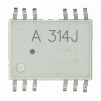
HCPL-314J-000E Avago Technologies US Inc., HCPL-314J-000E Datasheet - Page 3

HCPL-314J-000E
Manufacturer Part Number
HCPL-314J-000E
Description
OPTOCOUPLER GATE DRV 0.4A 16SOIC
Manufacturer
Avago Technologies US Inc.
Datasheet
1.HCPL-314J-000E.pdf
(14 pages)
Specifications of HCPL-314J-000E
Package / Case
16-SOIC (0.300", 7.50mm Width)
Voltage - Isolation
3750Vrms
Number Of Channels
2, Unidirectional
Propagation Delay High - Low @ If
300ns @ 8mA
Current - Dc Forward (if)
25mA
Input Type
DC
Output Type
Open Collector
Mounting Type
Surface Mount
Isolation Voltage
3750 Vrms
Maximum Fall Time
0.05 us
Maximum Forward Diode Current
25 mA
Minimum Forward Diode Voltage
1.2 V
Output Device
Logic Gate Photo IC
Configuration
2 Channel
Maximum Forward Diode Voltage
1.8 V
Maximum Reverse Diode Voltage
3 V
Maximum Power Dissipation
260 mW
Maximum Operating Temperature
+ 100 C
Minimum Operating Temperature
- 40 C
No. Of Channels
2
Optocoupler Output Type
Gate Drive
Input Current
12mA
Output Voltage
30V
Opto Case Style
SOIC
No. Of Pins
16
Common Mode Ratio
10 KV/uS
Rohs Compliant
Yes
Lead Free Status / RoHS Status
Lead free / RoHS Compliant
Lead Free Status / RoHS Status
Lead free / RoHS Compliant, Lead free / RoHS Compliant
Other names
516-1477-5
Available stocks
Company
Part Number
Manufacturer
Quantity
Price
Company:
Part Number:
HCPL-314J-000E
Manufacturer:
AVAGO
Quantity:
4 000
Company:
Part Number:
HCPL-314J-000E
Manufacturer:
AVAGO
Quantity:
30 000
Recommended Pb-Free IR Profile
Recommended reflow condition as per JEDEC Standard, J-STD-020 (latest revision). Non-Halide Flux should be used.
Regulatory Information
The HCPL-314J has been approved by the following organizations:
IEC/EN/DIN EN 60747-5-2
Approved under:
IEC 60747-5-5:1997 + A1:2002
EN 60747-5-2:2001 + A1:2002
DIN EN 60747-5-2 (VDE 0884
Teil 2):2003-01.
IEC/EN/DIN EN 60747-5-2 Insulation Characteristics
*
** Refer to the following figure for dependence of P
3
Description
Installation classification per DIN VDE 0110/1.89, Table 1
Climatic Classification
Pollution Degree (DIN VDE 0110/1.89)
Maximum Working Insulation Voltage
Input to Output Test Voltage, Method b*
Input to Output Test Voltage, Method a*
Highest Allowable Overvoltage
Safety-limiting values
- maximum values allowed in the event of a failure.
Insulation Resistance at T
(Transient Overvoltage t
for rated mains voltage ≤ 1000V
Case Temperature
Input Current**
Output Power**
Refer to the optocoupler section of the Isolation and Control Components Designer’s
Catalog, under Product Safety Regulations section, IEC/EN/DIN EN 60747-5-2, for a detailed
description of Method a and Method b partial discharge test profiles.
V
V
for rated mains voltage ≤ 150 V
for rated mains voltage ≤ 300 V
for rated mains voltage ≤ 600 V
t
t
IORM
m
IORM
m
=1 sec, Partial discharge < 5 pC
=10 sec, Partial discharge < 5 pC
x 1.875=V
x 1.6=V
PR
, Type and Sample Test,
PR
, 100% Production Test with
S
ini
, V
= 60 sec)
IO
= 500 V
rms
rms
rms
rms
S
and I
S
on ambient temperature.
UL
Approval under UL 1577, component recognition pro-
gram up to V
CSA
Approved under CSA Component Acceptance Notice
#5, File CA 88324.
Symbol
V
V
V
T
I
P
R
V
S,INPUT
S
IORM
PR
PR
IOTM
S, OUTPUT
S
ISO
= 5000 V
Characteristic
I - IV
I - IV
I - IV
I - III
55/100/21
2
1230
2306
1968
8000
175
400
1200
>10
9
800
700
600
500
400
300
200
100
0
0
rms
T
25
S
. File E55361.
– CASE TEMPERATURE – °C
50
75 100
Unit
V
V
V
V
°C
mA
mW
Ω
peak
peak
peak
peak
125
P
I
S
150 175
S
(mA)
(mW)
200


