SI8445-B-IS Silicon Laboratories Inc, SI8445-B-IS Datasheet
SI8445-B-IS
Specifications of SI8445-B-IS
Available stocks


Related parts for SI8445-B-IS


SI8445-B-IS Summary of contents
Page 1
... CSA component acceptance notice Description Silicon Lab's family of digital isolators are CMOS devices that employ an RF coupler to transmit digital information across an isolation barrier. Very high speed operation at low power levels is achieved. These parts are available in a 16-pin wide body SOIC package. Three speed grade options (1, 10, 150 Mbps) are available and achieve typical propagation delay of less than 10 ns ...
Page 2
Si8440/41/42/45 2 Rev. 0.62 ...
Page 3
T C ABLE O F ONTENTS Section 1. Electrical Specifications . . . . . . . . . . . . . . . . . . . . . . . . . . . . . . ...
Page 4
Si8440/41/42/45 1. Electrical Specifications Table 1. Electrical Characteristics ( –40 to 125 ºC) DD1 DD2 A Parameter Symbol High Level Input Voltage Low Level Input Voltage High Level Output Voltage Low ...
Page 5
Table 1. Electrical Characteristics (Continued –40 to 125 ºC) DD1 DD2 A Parameter Symbol Si844x-A Maximum Data Rate Minimum Pulse Width Propagation Delay t PHL Pulse Width Distortion |t - ...
Page 6
Si8440/41/42/45 Table 1. Electrical Characteristics (Continued –40 to 125 ºC) DD1 DD2 A Parameter Symbol For All Models Output Rise Time Output Fall Time Common Mode Transient CMTI Immunity Enable ...
Page 7
Table 2. Electrical Characteristics ( –40 to 125 ºC) DD1 DD2 A Parameter High Level Input Voltage Low Level Input Voltage High Level Output Voltage Low Level Output Voltage Input Leakage ...
Page 8
Si8440/41/42/45 Table 2. Electrical Characteristics (Continued 3 3 –40 to 125 ºC) DD1 DD2 A Parameter Si844x-A Maximum Data Rate Minimum Pulse Width Propagation Delay Pulse Width Distortion | ...
Page 9
Table 2. Electrical Characteristics (Continued 3 3 –40 to 125 ºC) DD1 DD2 A Parameter For All Models Output Rise Time Output Fall Time Common Mode Transient Immunity at Logic Low Output ...
Page 10
Si8440/41/42/45 Table 3. Electrical Characteristics ( –40 to 100 ºC) DD1 DD2 A Parameter High Level Input Voltage Low Level Input Voltage High Level Output Voltage Low Level Output Voltage Input ...
Page 11
Table 3. Electrical Characteristics (Continued 2 2 –40 to 100 ºC) DD1 DD2 A Parameter Si844x-A Maximum Data Rate Minimum Pulse Width Propagation Delay Pulse Width Distortion | PLH ...
Page 12
Si8440/41/42/45 Table 3. Electrical Characteristics (Continued 2 2 –40 to 100 ºC) DD1 DD2 A Parameter For All Models Output Rise Time Output Fall Time Common Mode Transient Immunity at Logic Low ...
Page 13
Table 4. Absolute Maximum Ratings Parameter Storage Temperature Ambient Temperature Under Bias Supply Voltage Input Voltage Output Voltage Output Current Drive Channel Lead Solder Temperature (10s) Maximum Isolation Voltage Note: Permanent device damage may occur if the above Absolute Maximum ...
Page 14
Si8440/41/42/45 Table 6. Regulatory Information CSA The Si84xx is certified under CSA Component Acceptance Notice. For more details, see File 232873. VDE The Si84xx is certified according to IEC 60747-5-2. For more details, see File 5006301-4880-0001. UL The Si84xx is ...
Page 15
Table 8. IEC 60664-1 (VDE 0884 Part 2) Ratings Parameter Basic isolation group Material Group Rated Mains Voltages < 150 V Rated Mains Voltages < 300 V Installation Classification Rated Mains Voltages < 400 V Table 9. IEC 60747-5-2 Insulation ...
Page 16
Si8440/41/42/45 Table 11. Thermal Characteristics Parameter IC Junction-to-Case Thermal Resistance IC Junction-to-Air Thermal Resistance Device Power Dissipation* *Note: The Si8440-C-IS is tested with V square wave. 200 175 162 150 125 100 Figure 3. Thermal ...
Page 17
Typical Performance Characteristics Data Rate (Mbps) Figure 4. Si8440/45 Typical V Current vs. Data Rate 5, 3.3, and 2.5 V Operation ...
Page 18
Si8440/41/42/ Falling Edge 7 6 Rising Edge 5 -40 - Temperature (Degrees C) Figure 9. Propagation Delay vs. Temperature 5 V Operation Falling Edge -40 -20 0 ...
Page 19
Application Information 3.1. Theory of Operation The operation of an Si8440 channel is analogous to that of an opto coupler, except an RF carrier is modulated instead of light. This simple architecture provides a robust isolated data path and ...
Page 20
Si8440/41/42/45 4. Layout Recommendations Dielectric isolation is a set of specifications produced by the safety regulatory agencies from around the world that describes the physical construction of electrical equipment that derives power from a high-voltage power system such as 100–240 ...
Page 21
... It is recommended that the enable inputs be connected to an external logic high or low level when the Si84xx is operating in noisy environments Connect (NC) replaces EN1 on Si8440/45. No Connect replaces EN2 on the Si8445. No Connects are not internally connected and can be left floating, tied to VDD, or tied to GND. 5. "Powered" state (P) is defined as 2.375 V < VDD < 5.5 V. ...
Page 22
... Outputs A3 and A4 are disabled and in high impedance state Outputs B1 and B2 are enabled Outputs B1 and B2 are disabled and in high impedance state. Si8445 — — Outputs B1, B2, B3, B4 are enabled. *Note not applicable Logic High Logic Low. 22 Table 13. Enable Input Truth Table Operation ...
Page 23
RF Radiated Emissions The Si8440 family uses a RF carrier frequency of approximately 2.1 GHz. This will result in a small amount of radiated emissions at this frequency and its harmonics. The radiation is not from the IC chip ...
Page 24
Si8440/41/42/45 4.5. RF Immunity and Common Mode Transient Immunity The Si8440 family has very high common mode transient immunity while transmitting data. This is typically measured by applying a square pulse with very fast rise/fall times between the isolated grounds. ...
Page 25
... Side 1 digital input or output. Digital Input Side 1 active high enable Si8440/45. Ground Side 1 ground. Ground Side 2 ground. Digital Input Side 2 active high enable Si8445. Digital I/O Side 2 digital input or output. Digital I/O Side 2 digital input or output. Digital Output Side 2 digital output. Digital Output Side 2 digital output ...
Page 26
... Si8441-A-IS 3 Si8441-B-IS 3 Si8441-C-IS 3 Si8442-A-IS 2 Si8442-B-IS 2 Si8442-C-IS 2 Si8445-B-IS 4 Note: All packages are Pb-free and RoHS compliant. Moisture sensitivity level is MSL3 with peak reflow temperature of °C 260 according to the JEDEC industry standard classifications, and peak solder temperature. 26 Number of Inputs Maximum Data V Side Rate ...
Page 27
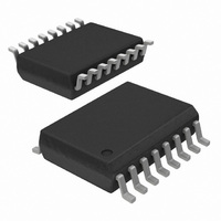
Package Outline: Wide Body SOIC Figure 17 illustrates the package details for the Quad-Channel Digital Isolator. Table 14 lists the values for the dimensions shown in the illustration. Table 14. Package Diagram Dimensions Figure 17. 16-Pin Wide Body SOIC ...
Page 28
... Added minimum and maximum values to the 5.0 V, 3.3 V, and 2.5 V electrical specifications in Table 1, Table 2, and Table 3, respectively. Revision 0.4 to Revision 0.5 Updated Block Diagram on page 1. Added Si8445 to various tables. Updated Table 6, “Package Characteristics,” on page 13. Updated Table 7, “Regulatory Information,” on page 14. ...
Page 29
N : OTES Si8440/41/42/45 Rev. 0.62 29 ...
Page 30
... Should Buyer purchase or use Silicon Laboratories products for any such unintended or unauthorized ap- plication, Buyer shall indemnify and hold Silicon Laboratories harmless against all claims and damages. Silicon Laboratories and Silicon Labs are trademarks of Silicon Laboratories Inc. Other products or brandnames mentioned herein are trademarks or registered trademarks of their respective holders. ...