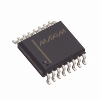
DS2188SN Maxim Integrated Products, DS2188SN Datasheet - Page 4

DS2188SN
Manufacturer Part Number
DS2188SN
Description
IC ATTEN JTR T1/CEPT IND 16-SOIC
Manufacturer
Maxim Integrated Products
Datasheet
1.DS2188SN.pdf
(10 pages)
Specifications of DS2188SN
Applications
*
Mounting Type
Surface Mount
Package / Case
16-SOIC (0.300", 7.5mm Width)
Lead Free Status / RoHS Status
Contains lead / RoHS non-compliant
Available stocks
Company
Part Number
Manufacturer
Quantity
Price
Company:
Part Number:
DS2188SN
Manufacturer:
TEXAS
Quantity:
519
Part Number:
DS2188SN
Manufacturer:
MAXIM/美信
Quantity:
20 000
PIN DESCRIPTION Table 1
CRYSTAL REQUIREMENTS
The DS2188 must have a crystal connected to the XTAL1 and XTAL2 pins. For T1 environments, the
frequency of this crystal should be 6.176 MHz. For CEPT environments, the frequency of this crystal
should be 8.192 MHz. Table 2 lists some suggested crystal manufacturers that are recommended for use
with the DS2188. Also, see DS2188 Application Note, “Operation at Speeds Greater than E1” for
additional information.
CRYSTAL MANUFACTURERS Table 2
PIN SYMBOL TYPE DESCRIPTION
10
11
12
13
14
15
16
1
2
3
4
5
6
7
8
9
MANUFACTURER
RRNEG
RRCLK
XTAL1
XTAL2
RRPOS
RNEG
RCLK
XTAL
RPOS
TEST
JAN Crystal
OUT
BDS
DJA
V
RST
V
BL
M-TRON
DD
SS
O
O
O
O
O
O
I
I
I
I
I
I
-
I
I
-
Disable Jitter Attenuation. When high, jittered data and clock at RPOS,
RNEG, and RCLK are passed directly to RRPOS, RRNEG, and RRCLK.
Receive Positive Data Input. Jittered data input. Sampled on the falling
edge of RCLK.
Receive Negative Data Input. Jittered data input. Sampled on the falling
edge of RCLK.
Receive Clock Input. Jittered input 1.544 MHz or 2.048 MHz clock.
Buffer Depth Select.
0 = 128 bits
1 = 32 bits
Test Input. In normal applications, this pin should be tied low.
Crystal Frequency Output. Buffered output of the 4X crystal connected
to XTAL1 and XTAL2.
Ground. 0.0V
Crystal Connections. In T1 environments, connect a 6.176 MHz crystal
to these pins. In CEPT environments, connect an 8.192 MHz crystal to
these pins.
Buffer Limit. Transitions high when the buffer fills or empties to within
either 4 bits (BDS=0) or 2 bits (BDS=1) of its capacity. Indicates that the
jitter at RCLK is greater than 120 UIpp (BDS=0) or 28 UIpp (BDS=1).
Reset. Negative-edge triggered; a high-low transition will recenter the
buffer. Activation of this pin may corrupt data through the DS2188.
Receive Reference Clock. Dejittered 1.544 MHz or 2.048 MHz clock.
Receive Reference Negative Data Output. Dejittered data output.
Updated on the rising edge of RRCLK.
Receive Reference Positive Data Output. Dejittered data output.
Updated on the rising edge of RRCLK.
Positive Supply. 5.0V
When tied high, used to verify free running frequency of XTAL.
6323-00, JC6A14
6323-00, JC8A14
4575-002
4575-001
PART #
4 of 10
FREQUENCY
6.176 MHz
8.192 MHz
6.176 MHz
8.192 MHz
DS2188


