NBSG16VSMNG ON Semiconductor, NBSG16VSMNG Datasheet - Page 9
NBSG16VSMNG
Manufacturer Part Number
NBSG16VSMNG
Description
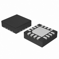
IC RCVR/DRIVER SIGE DIFF 16QFN
Manufacturer
ON Semiconductor
Type
Transceiverr
Datasheet
1.NBSG16VSMNR2G.pdf
(14 pages)
Specifications of NBSG16VSMNG
Applications
Instrumentation
Mounting Type
Surface Mount
Package / Case
16-TFQFN Exposed Pad
Logic Family
NBSG
Logic Type
Differential Receiver and Driver
Supply Voltage (max)
- 3.465 V or 3.465 V
Supply Voltage (min)
- 2.375 V or 2.375 V
Maximum Operating Temperature
85 C
Mounting Style
SMD/SMT
Minimum Operating Temperature
- 40 C
Number Of Lines (input / Output)
/ /
Supply Current
32 mA
Number Of Receivers
1
Number Of Transmitters
1
Number Of Transceivers
1
Receiver Signal Type
Differential
Transmitter Signal Type
Differential
Single Supply Voltage (typ)
2.5/3.3/-2.5/-3.3V
Single Supply Voltage (min)
2.375/-2.375V
Single Supply Voltage (max)
3.465/-3.465V
Dual Supply Voltage (typ)
Not RequiredV
Dual Supply Voltage (min)
Not RequiredV
Dual Supply Voltage (max)
Not RequiredV
Power Supply Requirement
Single
Operating Temp Range
-40C to 85C
Operating Temperature Classification
Industrial
Mounting
Surface Mount
Pin Count
16
Package Type
QFN EP
Lead Free Status / RoHS Status
Lead free / RoHS Compliant
Other names
NBSG16VSMNGOS


NOTE: Device will meet the specifications after thermal equilibrium has been established when mounted in a test socket or printed circuit
34. Measured using a 500 mV source, 50% duty cycle clock source. All loading with 50 W to V
35. t
36. V
37. Conditions include input amplitude of 500 mV and V
NOTE: Device will meet the specifications after thermal equilibrium has been established when mounted in a test socket or printed circuit
38. Measured using a 500 mV source, 50% duty cycle clock source. All loading with 50 W to V
39. t
40. V
41. Conditions include input amplitude of 500 mV and V
Table 10. AC CHARACTERISTICS for QFN−16
Table 11. AC CHARACTERISTICS for QFN−16
Symbol
Symbol
f
t
t
t
t
V
t
t
f
t
t
t
t
V
t
t
max
PLH
PHL
SKEW
JITTER
r
f
max
PLH
PHL
SKEW
JITTER
r
f
INPP
INPP
Spec in Figure 8).
Spec in Figure 9).
SKEW
SKEW
INPP(MAX)
INPP(MAX)
,
,
board with maintained transverse airflow greater than 500 lfpm. Electrical parameters are guaranteed only over the declared
operating temperature range. Functional operation of the device exceeding these conditions is not implied. Device specification limit
values are applied individually under normal operating conditions and not valid simultaneously.
= |t
= |t
Maximum Frequency
(See Figure 8) (Note 34)
Propagation Delay to
Output Differential
Duty Cycle Skew (Note 35)
RMS Random Clock Jitter
Peak−to−Peak Data Dependent Jitter
Input Voltage Swing/Sensitivity
(Differential Configuration) (Note 36)
Output Rise/Fall Times (20% − 80%)
@ 1 GHz
Maximum Frequency
(See Figure 9) (Note 38)
Propagation Delay to
Output Differential
Duty Cycle Skew (Note 39)
RMS Random Clock Jitter
Peak−to−Peak Data Dependent Jitter
Input Voltage Swing/Sensitivity
(Differential Configuration) (Note 40)
Output Rise/Fall Times (20% − 80%)
@ 1 GHz
PLH
PLH
cannot exceed V
cannot exceed V
(V
(V
(V
(V
(V
(V
(V
(V
−t
−t
CTRL
CTRL
CTRL
CTRL
CTRL
CTRL
CTRL
CTRL
PHL
PHL
| for a nominal 50% differential clock input waveform. See Figure 10.
| for a nominal 50% differential clock input waveform. See Figure 10.
= V
= V
= V
= V
= V
= V
= V
= V
Characteristic
Characteristic
CC
CC
CC
CC
CC
CC
CC
CC
− 2 V) D → Q, Q
− 1 V) D → Q, Q
− 2 V) Q, Q
− 1 V) Q, Q
− 2 V) D → Q, Q
− 1 V) D → Q, Q
− 2 V) Q, Q
− 1 V) Q, Q
CC
CC
− V
− V
f
f
EE
f
EE
f
in
in
in
in
< 10 Gb/s
< 10 GHz
< 10 Gb/s
< 10 GHz
(applicable only when V
(applicable only when V
(Note 41)
(Note 37)
CTRL
CTRL
Min
100
100
Min
100
100
V
V
10
75
25
22
10
75
30
30
CC
CC
http://onsemi.com
= V
= V
= 0 V; −3.0 V tV
= 0 V; V
−40°C
−40°C
CC
CC
CC
CC
TBD
TBD
Typ
140
135
Typ
140
135
0.5
0.5
12
50
45
12
45
40
3
3
− 2 V. Minimum output amplitude guarantee of 100 mV (see Output P−P
− 2 V. Minimum output amplitude guarantee of 100 mV (see Output P−P
− V
− V
9
EE
EE
EE
= −3.465 V to −3.0 V or V
2600
2600
Max
Max
180
180
180
180
20
70
60
20
55
50
3
2
t 2600 mV).
t 2600 mV).
EE
(Note 41)
(Note 37)
v −2.375 V or 2.375 V v V
Min
Min
100
100
100
100
10
75
25
22
10
75
30
30
25°C
25°C
TBD
TBD
Typ
Typ
CC
140
135
CC
140
135
0.5
0.5
12
50
45
12
45
40
3
3
−2.0 V. Input edge rates 40 ps (20% − 80%).
−2.0 V. Input edge rates 40 ps (20% − 80%).
CC
2600
2600
Max
Max
180
180
180
180
15
70
60
15
55
50
3
2
= 3.0 V to 3.465 V; V
(Note 41)
(Note 37)
Min
100
Min
100
10
80
75
25
22
10
80
75
30
30
CC
t 3.0 V; V
85°C
85°C
TBD
TBD
Typ
140
135
Typ
140
135
0.5
0.5
12
50
45
12
45
40
3
3
EE
EE
= 0 V
2600
2600
Max
Max
180
220
180
220
10
70
60
10
55
50
= 0 V
3
2
GHz
Unit
GHz
Unit
mV
mV
ps
ps
ps
ps
ps
ps
ps
ps
Related parts for NBSG16VSMNG
Image
Part Number
Description
Manufacturer
Datasheet
Request
R

Part Number:
Description:
Buffers & Line Drivers 2.5V/3.3V Multilevel
Manufacturer:
ON Semiconductor

Part Number:
Description:
ON Semiconductor [VOLTAGE REGULATOR]
Manufacturer:
ON Semiconductor
Datasheet:
Part Number:
Description:
357-036-542-201 CARDEDGE 36POS DL .156 BLK LOPRO
Manufacturer:
ON Semiconductor
Datasheet:
Part Number:
Description:
357-036-542-201 CARDEDGE 36POS DL .156 BLK LOPRO
Manufacturer:
ON Semiconductor
Datasheet:
Part Number:
Description:
357-036-542-201 CARDEDGE 36POS DL .156 BLK LOPRO
Manufacturer:
ON Semiconductor
Datasheet:
Part Number:
Description:
357-036-542-201 CARDEDGE 36POS DL .156 BLK LOPRO
Manufacturer:
ON Semiconductor
Datasheet:
Part Number:
Description:
357-036-542-201 CARDEDGE 36POS DL .156 BLK LOPRO
Manufacturer:
ON Semiconductor
Datasheet:
Part Number:
Description:
357-036-542-201 CARDEDGE 36POS DL .156 BLK LOPRO
Manufacturer:
ON Semiconductor
Datasheet:
Part Number:
Description:
357-036-542-201 CARDEDGE 36POS DL .156 BLK LOPRO
Manufacturer:
ON Semiconductor
Datasheet:
Part Number:
Description:
357-036-542-201 CARDEDGE 36POS DL .156 BLK LOPRO
Manufacturer:
ON Semiconductor
Datasheet:
Part Number:
Description:
357-036-542-201 CARDEDGE 36POS DL .156 BLK LOPRO
Manufacturer:
ON Semiconductor
Datasheet:
Part Number:
Description:
357-036-542-201 CARDEDGE 36POS DL .156 BLK LOPRO
Manufacturer:
ON Semiconductor
Datasheet:
Part Number:
Description:
Manufacturer:
ON Semiconductor
Datasheet: