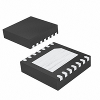
MAX4919BETD+T Maxim Integrated Products, MAX4919BETD+T Datasheet - Page 2

MAX4919BETD+T
Manufacturer Part Number
MAX4919BETD+T
Description
IC CTLR OVP/OCP BATT PWR 14-TDFN
Manufacturer
Maxim Integrated Products
Datasheet
1.MAX4915AEUKT.pdf
(11 pages)
Specifications of MAX4919BETD+T
Applications
*
Mounting Type
Surface Mount
Package / Case
14-TDFN Exposed Pad
Lead Free Status / RoHS Status
Lead free / RoHS Compliant
100mA/200mA/300mA Current-Limit Switches
with Low Shutdown Reverse Current
ABSOLUTE MAXIMUM RATINGS
IN, ON, FLAG, OUT to GND .....................................-0.3V to +6V
OUT Short Circuit to GND .................................Internally Limited
Continuous Power Dissipation (T
ELECTRICAL CHARACTERISTICS
(V
Stresses beyond those listed under “Absolute Maximum Ratings” may cause permanent damage to the device. These are stress ratings only, and functional
operation of the device at these or any other conditions beyond those indicated in the operational sections of the specifications is not implied. Exposure to
absolute maximum rating conditions for extended periods may affect device reliability.
2
Operating Voltage
Quiescent Current
Latchoff Current (Note 2)
Forward Shutdown Current
Reverse Shutdown Current
Forward Current Limit
Reverse Current Limit
ON Input Leakage
Undervoltage Lockout
Undervoltage-Lockout Hysteresis
On-Resistance
ON Input Logic-High Voltage
ON Input Logic-Low Voltage
FLAG Output Logic-Low Voltage
FLAG Output-High Leakage
Current
Thermal Shutdown
Thermal-Shutdown Hysteresis
DYNAMIC CHARACTERISTICS
Turn-On Time
IN
5-Pin SOT23 (derate 7.1mW/°C above +70°C)............571mW
6-Pin µDFN (derate 4.5mW/°C above +70°C)................358mW
_______________________________________________________________________________________
= +2.3V to +5.5V, T
PARAMETER
A
= -40°C to +85°C, unless otherwise noted. Typical values are at V
A
= +70°C)
SYMBOL
I
I
I
UVLO
LATCH
SHDN
SHDN
I
R
I
FWD
V
V
REV
V
I
ON
IN
Q
IH
IL
V
switch on
V
M AX 4915B/M AX 4917B ( l atchoff ver si ons)
V
V
MAX4914B, V
MAX4915_, V
MAX4917_, V
MAX4914B, V
MAX4915_, V
MAX4917_, V
V
Rising edge
T
T
MAX4914B/MAX4915B/MAX4917B
MAX4915A/MAX4917A
MAX4914B/MAX4915B/MAX4917B
MAX4915A/MAX4917A
I
V
V
C
S IN K
ON
A
A
ON
ON
ON
ON
ON
ON
L
= +25°C, I
= - 40° C to + 85°C , I
= 0.1µF (Note 3)
= V
= 0, V
= V
= 0, V
= V
= V
from low to high; I
= 1m A
IN
IN
IN
IN
, after an over cur r ent faul t M AX 4914B/
, I
OUT
OUT
or GND
= V
OUT
OUT
OUT
OUT
OUT
OUT
OUT
OUT
FLAG
= +5.5V, V
= 0, V
CONDITIONS
= 0,
= GND
= GND
- V
- V
= 95mA
= GND
- V
= +5.5V
IN
IN
IN
Operating Temperature Range ...........................-40°C to +85°C
Junction Temperature ......................................................+150°C
Storage Temperature Range .............................-65°C to +150°C
Lead Temperature (soldering, 10s) .................................+300°C
IN
OU T
OUT
≥ 0.5V
≥ 0.5V
≥ 0.5V
= +5.5V
V
V
IN
IN
IN
= 95m A
= 10mA,
= +2.3V
= +2.3V to +5.0V
= +5.0V to +5.5V
IN
= +3.3V, T
1.75
MIN
100
200
300
2.3
2.0
1.4
-1
A
= +25°C.) (Note 1)
+150
TYP
0.01
0.01
100
100
0.2
80
15
8
MAX
2.25
120
160
150
300
450
150
300
450
5.5
0.4
0.5
0.8
0.4
0.4
+1
17
1
1
1
UNITS
mA
mA
mV
µA
µA
µA
µA
µA
µA
°C
°C
µs
Ω
V
V
V
V
V


