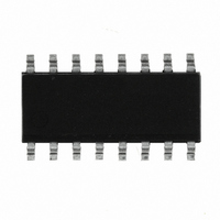
LX5261CDP Microsemi Analog Mixed Signal Group, LX5261CDP Datasheet - Page 4

LX5261CDP
Manufacturer Part Number
LX5261CDP
Description
IC REG SCSI 27LINE LVD 16SOIC
Manufacturer
Microsemi Analog Mixed Signal Group
Datasheet
1.LX5261CDP.pdf
(6 pages)
Specifications of LX5261CDP
Applications
*
Mounting Type
Surface Mount
Package / Case
16-SOIC (3.9mm Width)
Lead Free Status / RoHS Status
Contains lead / RoHS non-compliant
Copyright © 2000
Rev. 1.0c, 2005-02-08
LVD SCSI with Resistor Stack
The LX5261 is used with a LVD resistor network (475Ω, 121Ω, 475Ω) to meet LVD SCSI performance. Connecting the top side of the
LVD resistor network to the 1.75V regulated output (V
output (V
voltage required by the SPI-2 through SPI-4 SCSI specification (see Figure 2. below). The LX5261 is designed to drive up to 27 LVD
pairs.
TM
REG2
, pin 3) provides the correct bias voltage, differential impedance, common mode differential impedance, and common mode
+
+
-
-
200mA source/sink
200mA source/sink
1.75V +/- 0.05V
0.75V +/- 0.05V
11861 Western Avenue, Garden Grove, CA. 92841, 714-898-8121, Fax: 714-893-2570
VTERM
GND
4.7uF
4.7uF
6
3
2
4
VOUT1
VOUT2
A P P L I C A T I O N I N F O R M A T I O N
Figure 2 – LX5261 with LVD Resistor Stack
27
27
Figure 1 – LX5261 Block Diagram
Reference
Reference
Reference
475
1%
1.75V
0.75V
475
1%
1.3V
Integrated Products Division
B L O C K D I A G R A M
REG1,
121
1%
®
Microsemi
pin 6), and the bottom side of the LVD resistor network to the 0.75 regulated
LVD Pairs
Ln+
Ln-
1 of 27
27-Line LVD SCSI Source/Sink Regulator
+
+
+
-
-
-
Differential Impedance
Differential Bias Voltage
Common Mode Impedance
Common Mode Voltage
200mA source/sink
1.3V +/- 0.1V
200mA source/sink
1.75V +/- 0.05V
0.75V +/- 0.05V
Parameter
P
RODUCTION
LX5261
7
6
3
107.3
112.9
1.25
237
DIFSENS
VOUT1
VOUT2
D
ATA
SCSI Standard
100 to 110
100 to 125
100 to 300
1.2 to 1.3
S
HEET
Units
ohm
mV
ohm
V
LX5261
Page 4


