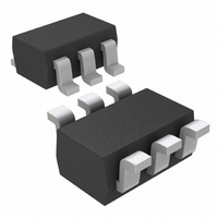
MAX4840AEXT+T Maxim Integrated Products, MAX4840AEXT+T Datasheet - Page 5

MAX4840AEXT+T
Manufacturer Part Number
MAX4840AEXT+T
Description
IC CTLR OVP 5.8V SC70-6
Manufacturer
Maxim Integrated Products
Type
Overvoltage Protection Controllerr
Datasheet
1.MAX4840EXTT.pdf
(11 pages)
Specifications of MAX4840AEXT+T
Applications
Cell Phones, Digital Cameras, Media Players
Mounting Type
Surface Mount
Package / Case
SC-70-6, SC-88, SOT-363
Number Of Voltages Monitored
1
Monitored Voltage
3.25 V to 5.8 V
Undervoltage Threshold
3.25 V
Overvoltage Threshold
5.8 V
Output Type
Active Low, Open Drain
Manual Reset
Not Resettable
Watchdog
No Watchdog
Battery Backup Switching
No Backup
Power-up Reset Delay (typ)
50 ms
Supply Voltage (max)
28 V
Supply Voltage (min)
1.2 V
Supply Current (typ)
80 uA
Maximum Power Dissipation
245 mW
Maximum Operating Temperature
+ 85 C
Mounting Style
SMD/SMT
Minimum Operating Temperature
- 40 C
Power Fail Detection
No
Lead Free Status / RoHS Status
Lead free / RoHS Compliant
Other names
MAX4840AEXT+T
MAX4840AEXT+TTR
MAX4840AEXT+TTR
Figure 1. Startup Timing Diagram
Figure 3. Power-Up Overvoltage Timing Diagram
I
( ) MAX4842A
GATE
V
0V
IN
( ) MAX4842A
V
V
FLAG
GATE
V
0V
IN
PIN
1
2
3
4
5
6
V
OVLO
V
UVLO
t
OVP
_______________________________________________________________________________________
Overvoltage-Protection Controllers with
t
START
NAME
GATE
FLAG
GND
N.C.
EN
IN
80%
0.3V
t
GON
Input. IN is both the power-supply input and the overvoltage sense input. Bypass IN to GND with
a 1µF capacitor or larger.
Ground
Fault Indication Output, Open-Drain, Active Low. FLAG is asserted low during undervoltage-
lockout and overvoltage-lockout conditions. FLAG is deasserted during normal operation.
Gate-Drive Output. GATE is the output of an on-chip charge pump. When V
GATE is driven high to turn on the external n-channel MOSFET(s).
No Connection. Not internally connected for µDFN package. Connected to ground for SC70
6-pin package; connect to ground or leave unconnected.
Device Enable Input, Active Low. Drive EN low or connect to ground to allow normal device
operation. Drive EN high to turn off the external MOSFET.
5V (4V)
8V (6V)
t
BLANK
2.4V
8V (6V)
Figure 2. Shutdown Timing Diagram
Figure 4. Disable Timing Diagram
5V (4V)
( ) MAX4842A
V
V
FLAG
GATE
V
IN
V
GATE
V
FUNCTION
EN
V
OVLO
1.5V
t
GOFF
t
DIS
Status FLAG
0.3V
Timing Diagrams
0.3V
t
Pin Description
FLAG
UVLO
< V
0.4V
IN
< V
OVLO
8V (6V)
,
5


