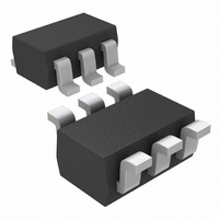
MAX4840EXT+T Maxim Integrated Products, MAX4840EXT+T Datasheet - Page 7

MAX4840EXT+T
Manufacturer Part Number
MAX4840EXT+T
Description
IC CTLR OVP 5.8V SC70-6
Manufacturer
Maxim Integrated Products
Type
Overvoltage Protection Controllerr
Datasheet
1.MAX4840EXTT.pdf
(11 pages)
Specifications of MAX4840EXT+T
Applications
Cell Phones, Digital Cameras, Media Players
Mounting Type
Surface Mount
Package / Case
SC-70-6, SC-88, SOT-363
Lead Free Status / RoHS Status
Lead free / RoHS Compliant
Other names
MAX4840EXT+T
MAX4840EXT+TTR
MAX4840EXT+TTR
The MAX4838A/MAX4840A/MAX4842A can be used
with either a single MOSFET configuration as shown in
the Typical Operating Circuit, or can be configured with
a back-to-back MOSFET as shown in Figure 7. The
back-to-back configuration has almost zero reverse
current when the input supply is below the output.
If reverse current leakage is not a concern, a single
MOSFET can be used. This approach has half the loss
of the back-to-back configuration when used with simi-
lar MOSFET types, and is a lower cost solution. Note
that if the input is actually pulled low, the output is
pulled low as well due to the parasitic body diode in the
MOSFET. If this is a concern, then the back-to-back
configuration should be used.
The MAX4838A/MAX4840A/MAX4842A are designed for
use with either a single n-channel MOSFET or dual back-
to-back n-channel MOSFETs. In most situations,
MOSFETs with R
well. If the input supply is near the UVLO maximum of
Figure 6. State Diagram
V
IN
< UVLO
Applications Information
DS(ON)
_______________________________________________________________________________________
Overvoltage-Protection Controllers with
GATE DRIVEN HIGH
TIMER STARTS
OVLO CHECK
FLAG = HIGH
specified for a V
FLAG = LOW
FLAG = LOW
FLAG = LOW
GATE HIGH
COUNTING
STANDBY
STARTUP
GATE = 0
GATE = 0
MOSFET Configuration
ON
V
V
t = 50ms
t = 50ms
IN
IN
> UVLO
< OVLO
MOSFET Selection
GS
of 4.5V work
V
IN
> OVLO
3.5V, consider using a MOSFET specified for a lower
V
FET to withstand the full 28V IN range of all devices.
Table 1 shows a selection of MOSFETs appropriate for
use with the MAX4838A/MAX4840A/MAX4842A.
For most applications, bypass IN to GND with a 1µF
ceramic capacitor. If the power source has significant
inductance due to long lead length, take care to pre-
vent overshoots due to the LC tank circuit and provide
protection if necessary to prevent exceeding the 30V
absolute maximum rating on IN.
The MAX4838A/MAX4840A/MAX4842A provide protec-
tion against voltage faults up to 28V, but this does not
include negative voltages. If negative voltages are a con-
cern, connect a Schottky diode from IN to GND to clamp
negative input voltages.
ESD performance depends on a number of conditions.
The MAX4838A/MAX4840A/MAX4842A are specified
for ±15kV typical ESD resistance on IN when IN is
bypassed to ground with a 1µF ceramic capacitor.
Contact Maxim for a reliability report that documents
test setup, methodology, and results.
Figure 8 shows the Human Body Model, and Figure 9
shows the current waveform it generates when dis-
charged into a low impedance. This model consists of
a 100pF capacitor charged to the ESD voltage of inter-
est, which is then discharged into the device through a
1.5kΩ resistor.
Figure 7. Back-to-Back External MOSFET Configuration
GS
0 TO 28V
INPUT
voltage. Also, the V
1µF
1
6
2
IN
EN
GND
MAX4838A
MAX4840A
MAX4842A
IN Bypass Considerations
DS
Status FLAG
FLAG
should be 30V for the MOS-
GATE
ESD Test Conditions
Human Body Model
4
3
NMOS
NOTE: EN AND PULLUP
RESISTOR ON MAX4838A/
MAX4840A/MAX4842A ONLY.
V
IO
OUTPUT
7


