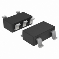
MAX828EUKG ON Semiconductor, MAX828EUKG Datasheet

MAX828EUKG
Specifications of MAX828EUKG
MAX828EUKGOS
MAX828EUKGOSTR
Available stocks
Related parts for MAX828EUKG
MAX828EUKG Summary of contents
Page 1
... C GND (Top View) ORDERING INFORMATION Device Package Shipping MAX828EUK TSOP−5 3000 Tape/Reel MAX828EUKG TSOP−5 3000 Tape/Reel (Pb−Free) MAX829EUK TSOP−5 3000 Tape/Reel MAX829EUKG TSOP−5 3000 Tape/Reel (Pb−Free) †For information on tape and reel specifications, including part orientation and tape sizes, please refer to our Tape and Reel Packaging Specifications Brochure, BRD8011/D ...
Page 2
MAXIMUM RATINGS* Rating Á Á Á Á Á Á Á Á Á Á Á Á Á Á Á Á Á Á Á Á Input Voltage Range (V to GND) in Á Á Á Á Á Á Á Á Á Á ...
Page 3
Figure 20 Test Setup 1.0 1.5 2.0 2.5 3.0 3.5 4 SUPPLY VOLTAGE (V) in Figure 2. Output Resistance vs. Supply Voltage MAX828 90 Figure 20 Test Setup V ...
Page 4
Figure 20 Test Setup 350 300 V = −4.0 V out 250 200 V = −2.5 V out 150 100 V = −1.5 V ...
Page 5
Figure 20 Test Setup −1 2 −2 3.3 V −3.0 in −4 5 −5.0 −6 OUTPUT CURRENT (mA) out Figure 14. Output Voltage ...
Page 6
OSC MAX828 3.3 mF MAX829 Figure 20. Test Setup/Voltage Inverter ...
Page 7
Capacitor Selection In order to maintain the lowest output resistance and output ripple voltage recommended that low ESR capacitors be used. Additionally, larger values of C lower the output resistance and larger values of C reduce output voltage ...
Page 8
The MAX828 / 829 primary function is a voltage inverter. The device will convert 5.0 V into −5.0 V with light loads. Two capacitors are required for the inverter to function. A third capacitor, the input bypass capacitor, may be ...
Page 9
A −4.0 −5.0 −6.0 −7.0 −8.0 −9.0 −10 OUTPUT CURRENT (mA) out Figure 28. Cascade Load Regulation, Output Voltage vs. Output Current MAX828 Curve V (V) R (W) in out A 3.0 ...
Page 10
Curve single device can be used to construct a negative voltage tripler. The output voltage is approximately equal to −3V the forward voltage drop of each external diode. The performance characteristics for the ...
Page 11
Curve single device can be used to construct a positive voltage doubler. The output voltage is approximately equal to 2V the forward voltage drop of each external diode. The performance characteristics for the above converter are ...
Page 12
Curve single device can be used to construct a positive voltage tripler. The output voltage is approximately equal to 3V the forward voltage drop of each external diode. The performance characteristics for the ...
Page 13
Curve Figure 42. Paralleling Devices for Increased Negative Output Current An increase in converter output current capability with a reduction in output resistance can be obtained by paralleling two or more devices. The output ...
Page 14
−V out Figure 45. External Switch for Increased Negative Output Current The output current capability of the MAX828 and MAX829 can be extended beyond 600 mA with the addition of two external switch transistors and ...
Page 15
Figure 48. Positive Output Voltage Doubler with High Current Capability The MAX828/829 can be configured to produce a positive output voltage doubler with current capability in excess of 500 mA. This is ...
Page 16
All of the previously shown converter circuits have only single outputs. Applications requiring multiple outputs can be constructed by incorporating combinations of the former circuits. The converter shown above combines Figures 24 and 36 to form a negative output inverter ...
Page 17
... H *For additional information on our Pb−Free strategy and soldering details, please download the ON Semiconductor Soldering and Mounting Techniques Reference Manual, SOLDERRM/D. ON Semiconductor and are registered trademarks of Semiconductor Components Industries, LLC (SCILLC). SCILLC reserves the right to make changes without further notice to any products herein ...


