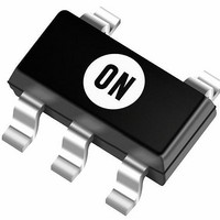
MAX829EUK ON Semiconductor, MAX829EUK Datasheet - Page 16

MAX829EUK
Manufacturer Part Number
MAX829EUK
Description
IC INVERTER CHARGE PUMP SOT23-5
Manufacturer
ON Semiconductor
Type
Switched Capacitor (Charge Pump), Doubler, Invertingr
Datasheet
1.MAX829EUK.pdf
(17 pages)
Specifications of MAX829EUK
Internal Switch(s)
Yes
Synchronous Rectifier
No
Number Of Outputs
1
Voltage - Output
-1.15 ~ -5.5 V, 2.3 ~ 11 V
Current - Output
50mA
Frequency - Switching
19kHz ~ 54kHz
Voltage - Input
1.15 ~ 5.5 V
Operating Temperature
-40°C ~ 85°C
Mounting Type
Surface Mount
Package / Case
TSOT-23-5, TSOT-5, TSOP-5
Power - Output
313mW
Function
Inverting
Output Voltage
- 5.5 V to - 1.15 V
Output Current
100 mA
Maximum Operating Temperature
+ 150 C
Mounting Style
SMD/SMT
Lead Free Status / RoHS Status
Contains lead / RoHS non-compliant
Other names
MAX829EUKOS
Available stocks
Company
Part Number
Manufacturer
Quantity
Price
Company:
Part Number:
MAX829EUK
Manufacturer:
MAXIM
Quantity:
5 321
Company:
Part Number:
MAX829EUK
Manufacturer:
MAX
Quantity:
356
Company:
Part Number:
MAX829EUK+T
Manufacturer:
Intersil
Quantity:
230
Company:
Part Number:
MAX829EUK+T
Manufacturer:
MAXIN
Quantity:
10
Part Number:
MAX829EUK+T
Manufacturer:
MAXIM/美信
Quantity:
20 000
Part Number:
MAX829EUKG
Manufacturer:
ON/安森美
Quantity:
20 000
constructed by incorporating combinations of the former circuits. The converter shown above combines Figures 24 and 36 to form
a negative output inverter with a positive output doubler. Different combinations of load regulation are shown below. In
Figures 52 and 53 the positive doubler has a constant I
and 55 the negative inverter has the constant I
All of the previously shown converter circuits have only single outputs. Applications requiring multiple outputs can be
−4.0
−4.5
−5.0
−4.0
−4.5
−5.0
9.5
9.0
8.5
9.5
9.0
8.5
0
0
I
Figure 52. Negative Inverter Load Regulation,
out
Negative Inverter
I
Figure 54. Positive Doubler Load Regulation,
Negative Inverter
Output Voltage vs. Output Current, MAX828
out
Output Voltage vs. Output Current, MAX828
, NEGATIVE INVERTER OUTPUT CURRENT (mA)
, POSITIVE DOUBLER OUTPUT CURRENT (mA)
10
10
Figure 56. Inverter Circuit Board Layout, Top View Copper Side
GND
Negative Inverter I
T
Negative Inverter R
T
V
A
A
in
= 25°C
= 25°C
Positive Doubler
I
Positive Doubler
R
out
out
20
20
= 15 mA
= 21.4 W
C
out
+
out
3
Inverter Size = 0.5 in x 0.2 in
out
Area = 0.10 in
= 15 mA and the positive doubler has the variable load.
= 15 mA
= 28.8 W
MAX828, MAX829
out
http://onsemi.com
IC1
= 15 mA while the negative inverter has the variable load. In Figures 54
0.5 ″
30
30
16
2
, 64.5 mm
C
+
1
−4.0
−4.5
−5.0
−4.0
−4.5
−5.0
9.5
9.0
8.5
9.5
9.0
8.5
0
0
2
I
Figure 53. Negative Inverter Load Regulation,
out
Negative Inverter
Negative Inverter
C
I
Figure 55. Positive Doubler Load Regulation,
Output Voltage vs. Output Current, MAX829
out
Output Voltage vs. Output Current, MAX829
+
2
, NEGATIVE INVERTER OUTPUT CURRENT (mA)
, POSITIVE DOUBLER OUTPUT CURRENT (mA)
10
10
−V
GND
out
Negative Inverter R
T
Negative Inverter I
T
A
A
= 25°C
= 25°C
Positive Doubler
I
Positive Doubler
R
out
out
20
20
= 15 mA
= 20 W
out
out
= 15 mA
= 28 W
30
30


