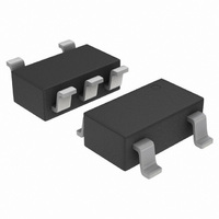
NCP1403SNT1 ON Semiconductor, NCP1403SNT1 Datasheet

NCP1403SNT1
Specifications of NCP1403SNT1
Available stocks
Related parts for NCP1403SNT1
NCP1403SNT1 Summary of contents
Page 1
... Digital Still Camera • Handheld Games • Hand-held Instrument © Semiconductor Components Industries, LLC, 2007 May, 2007 - Rev NCP1403SNT1 NCP1403SNT1G †For information on tape and reel specifications, 1 http://onsemi.com 5 1 TSOP-5 SN SUFFIX CASE 483 MARKING DIAGRAM AND PIN CONNECTIONS ...
Page 2
VDD Enable Figure 1. Typical Step-Up Application Circuit ...
Page 3
PIN FUNCTION DESCRIPTIONS Pin Symbol 1 CE Chip Enable Pin 1. The chip is enabled if a voltage which is equal to or greater than 0 applied. 2. The chip is disabled if a voltage which is less ...
Page 4
ELECTRICAL CHARACTERISTICS Characteristic ON/OFF TIMING CONTROL Minimum Off Time ( Maximum On Time (Current not asserted) Maximum Duty Cycle Minimum Startup Voltage ( mA) OUT Minimum Startup Voltage Temperature ...
Page 5
16 OUT = OUT 16 25°C A Figure 1 15.5 15.0 14.5 3.6 V 1.8 V 2.4 V 3.0 V 14.0 13.5 13 ...
Page 6
V , INPUT VOLTAGE (V) IN Figure 10. No Load Input Current versus Input Voltage ...
Page 7
T , AMBIENT TEMPERATURE (°C) A Figure 16. Maximum Switch On Time 170 150 130 110 -50 - AMBIENT TEMPERATURE ...
Page 8
OUT OUT V/div OUT V/div 3 V/div ...
Page 9
Operation The NCP1403 is monolithic DC-DC switching converter optimized for single Lithium or two cells AA/AAA size batteries powered portable products. The NCP1403 device consists of startup circuit, chip enable circuit, PFM comparator, voltage reference, PFM on/off timing control circuit, ...
Page 10
External Component Selection Inductor The NCP1403 is designed to work well with a range of inductance values, the actual inductance value depends on the specific application, output current, efficiency, and output ripple voltage. For step up conversion, the device works ...
Page 11
Output Voltage Higher than 15 V NCP1403 can be used to generate output voltage higher than adding an external high voltage N-Channel MOSFET in series with the internal MOSFET switch as shown in Figure 33. The drain-to-source ...
Page 12
Power Signal Traces Low resistance conducting paths should be used for the power carrying traces to reduce power loss improve efficiency (short and thick traces for connecting the inductor L can also reduce stray inductance). Besides, the ...
Page 13
Figure 29. Step-Up Converter Demonstration Board Top Layer Copper Figure 30. Step-Up Converter Demonstration Board Bottom Layer Copper Figure 31. Step-Up Converter Demonstration Board Top Layer Component Silkscreen http://onsemi.com NCP1403 13 ...
Page 14
... D1 ON Semiconductor C1 Kemet Electronics Corp. C2 Kemet Electronics Corp 2 5 CD43-470KC, Sumida C1: T494A106K010AS, Kemet C2: EMK107BJ104MA, Taiyo Yuden C3: GMK316F225ZG, Taiyo Yuden C4: T494D336K025AS, Kemet D1, D2, D3: MBR0520LT1, ON Semiconductor Figure 32. Positive-to-Negative Output Converter for Negative LCD Bias VDD 3 L: CD43-470KC, Sumida C1: T494A106K010AS, Kemet C2: T494D226K035AS, Kemet ...
Page 15
... Figure 34. Step-down DC-DC Converter with 1.6 V Output Voltage for DSP Circuit FB1 C 750 pF to 2000 pF VDD R FB2 L: CD43-470KC, Sumida C1: T494A106K010AS, Kemet C2, C4: T494D106K020AS, Kemet C3: GMK316F225ZG, Taiyo Yuden D1, D2, D3: MBR0520LT1, ON Semiconductor Figure 35. Step-Up DC-DC Converter with 30 V Output Voltage NCP1403 Q1 MGSF1P02LT1 R GS 820 MBR0520LT1 NCP1403 GND 2 ...
Page 16
... IN C1 750 2000 JPI 1 OFF VDD 3 L1: CD43-470KC, Sumida C1: T494A106K010AS, Kemet C2, C5: T494C226K020AS, Kemet C3: UMK107B102KZ, Taiyo Yuden C4: TMK316BJ225ML, Taiyo Yuden D1, D2, D3: MBR0520LT1, ON Semiconductor R1: 390 kW Figure 37. +15 V, -15 V Outputs Converter for LCD Bias Supply R2 NCP1403 2 MMSD914T1 Q1 LX MGSF1N03T1 NTHS5402T1 D1 MMSD914T1 NCP1403 GND V OUT [ * 0 ...
Page 17
... JPI 1 OFF VDD 3 L1: CD43-470KC, Sumida C1, C2: T494A106K010AS, Kemet C3: UMK107B102KZ, Taiyo Yuden C4, C5: TMK316BJ225ML, Taiyo Yuden C6, C7: T494C226K020AS, Kemet D1, D2, D3, D4, D5: MBR0520LT1, ON Semiconductor R1: 390 kW Figure 38. +15 V, -7.5 V Outputs Converter for CCD Supply Circuit R2 NCP1403 MBR0520LT1 D3 C5 MBR0520LT1 2 2.2 mF MBR0520LT1 MBR0520LT1 NCP1403 ...
Page 18
... C 0.05 H *For additional information on our Pb-Free strategy and soldering details, please download the ON Semiconductor Soldering and Mounting Techniques Reference Manual, SOLDERRM/D. The product described herein (NCP1403), may be covered by the following U.S. patents: 6,518,834. There may be other patents pending. ON Semiconductor and are registered trademarks of Semiconductor Components Industries, LLC (SCILLC). SCILLC reserves the right to make changes without further notice to any products herein ...


