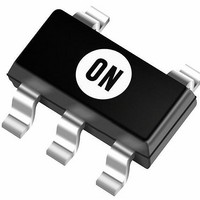
NCP1400ASN50T1 ON Semiconductor, NCP1400ASN50T1 Datasheet

NCP1400ASN50T1
Specifications of NCP1400ASN50T1
Available stocks
Related parts for NCP1400ASN50T1
NCP1400ASN50T1 Summary of contents
Page 1
NCP1400A 100 mA, Fixed Frequency PWM Step−Up Micropower Switching Regulator The NCP1400A series are micropower step− converters that are specifically designed for powering portable equipment from one or two cell battery packs. These devices are designed to ...
Page 2
... V NCP1400ASN45T1G 4.5 V NCP1400ASN50T1 5.0 V NCP1400ASN50T1G 5.0 V NOTE: The ordering information lists seven standard output voltage device options. Additional devices with output voltage ranging from 1 5 100 mV increments can be manufactured. Contact your ON Semiconductor representative for availability. †For information on tape and reel specifications, including part orientation and tape sizes, please refer to our Tape and Reel Packaging Specifications Brochure, BRD8011/D ...
Page 3
ABSOLUTE MAXIMUM RATINGS Rating Power Supply Voltage (Pin 2) Input/Output Pins LX (Pin 5) LX Peak Sink Current CE (Pin 1) Input Voltage Range Input Current Range Thermal Resistance Junction to Air Operating Ambient Temperature Range (Note 2) Operating Junction ...
Page 4
ELECTRICAL CHARACTERISTICS (continued) (For all values T Characteristic CE (PIN 1) CE Input Voltage ( 0.96) OUT SET High State, Device Enabled Low State, Device Disabled CE Input Current (Note 6) High State, Device Enabled (V = ...
Page 5
... Figure 3. NCP1400ASN30T1 Output Voltage 100 3 2 NCP1400ASN19T1 25° 100 0 Figure 5. NCP1400ASN19T1 Efficiency vs. 100 NCP1400ASN50T1 25° 100 0 Figure 7. NCP1400ASN50T1 Efficiency vs. http://onsemi.com OUTPUT CURRENT (mA) O vs. Output Current OUTPUT CURRENT (mA) O Output Current OUTPUT CURRENT (mA) ...
Page 6
... T A Figure 11. NCP1400ASN19T1 V 1.0 0.8 0.6 0.4 NCP1400ASN50T1 0 5 0.96 OUT 0 75 100 −50 − Voltage Limit Figure 13. NCP1400ASN50T1 V LX http://onsemi.com AMBIENT TEMPERATURE (° AMBIENT TEMPERATURE (°C) Voltage Limit LX vs. Temperature AMBIENT TEMPERATURE (°C) Voltage Limit LX vs. Temperature ...
Page 7
... OUT Open−loop Test 100 −50 −25 Figure 17. NCP1400ASN50T1 Oscillator 100 NCP1400ASN50T1 V 50 OUT Open−loop Test 100 −50 −25 Figure 19. NCP1400ASN50T1 Maximum Duty http://onsemi.com AMBIENT TEMPERATURE (°C) A vs. Temperature = 5 0. AMBIENT TEMPERATURE (°C) A Frequency vs. Temperature = 5 0. AMBIENT TEMPERATURE (°C) A Cycle vs ...
Page 8
... AMBIENT TEMPERATURE (°C) A Figure 21. NCP1400ASN50T1 Startup/Hold Voltage vs. Temperature 260 220 180 140 NCP1400ASN50T1 100 75 100 −50 − AMBIENT TEMPERATURE (°C) A Figure 23. NCP1400ASN50T1 LX Pin On−State Current vs. Temperature 5.0 4.0 3.0 2.0 NCP1400ASNXXT1 V = 0 25° 4.5 5.0 5.5 1.5 2.0 2.5 ...
Page 9
... NCP1400ASN19T1 OUT 60 25° Figure 29. NCP1400ASN19T1 Ripple Voltage 80 NCP1400ASN50T1 OUT 25° 0 100 0 20 Figure 31. NCP1400ASN50T1 Ripple Voltage http://onsemi.com 9 V start V hold NCP1400ASN30T1 OUT T = 25° OUTPUT CURRENT ( 100 I , OUTPUT CURRENT (mA) O vs. Output Current 100 ...
Page 10
OUT 2.0 V/div mV/div, AC coupled OUT 100 ...
Page 11
... Output voltage monitor pin and also the power supply pin for the device. No internal connection to this pin. Ground pin. External inductor connection pin to power switch drain. http://onsemi.com 5.0 V (AC coupled), 50 mV/div OUT 3 Figure 39. NCP1400ASN50T1 Load Transient Response LIMITER LX DRIVER POWER SWITCH PWM 180 kHz LX 5 ...
Page 12
Operation The NCP1400A series are monolithic power switching regulators optimized for applications where power drain must be minimized. These devices operate as fixed frequency, voltage mode boost regulator and is designed to operate in the discontinuous conduction mode. Potential applications ...
Page 13
Step−up Converter Design Equations General step−up DC−DC converter designed to operate in discontinuous conduction mode can be defined by: Calculation Equation Á Á Á Á Á Á Á Á Á Á Á Á Á Á Á Á Á Á D ...
Page 14
An evaluation board of NCP1400A has been made in the small size and is shown in Figures 42 and 43. Please contact your Figure 42. NCP1400A PWM Step−up DC−DC Converter Evaluation Board Silkscreen Figure ...
Page 15
... Schottky Diode Semiconductor Corp. Á Á Á Á Á Á Á Á Á Á Á Á Á Á Á Á Á Á Á Á Á Á ...
Page 16
... H *For additional information on our Pb−Free strategy and soldering details, please download the ON Semiconductor Soldering and Mounting Techniques Reference Manual, SOLDERRM/D. ON Semiconductor and are registered trademarks of Semiconductor Components Industries, LLC (SCILLC). SCILLC reserves the right to make changes without further notice to any products herein ...


