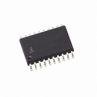
EL7564CM Intersil, EL7564CM Datasheet

EL7564CM
Specifications of EL7564CM
Available stocks
Related parts for EL7564CM
EL7564CM Summary of contents
Page 1
... CAUTION: These devices are sensitive to electrostatic discharge; follow proper IC Handling Procedures. 1-888-INTERSIL or 1-888-352-6832 All other trademarks mentioned are the property of their respective owners. EL7564 May 9, 2005 FN7297.3 | Intersil (and design registered trademark of Intersil Americas Inc. Copyright Intersil Americas Inc. 2003, 2005. All Rights Reserved ...
Page 2
... Ordering Information PART NUMBER PACKAGE EL7564CM 20-Pin SO (0.300”) EL7564CM-T13 20-Pin SO (0.300”) EL7564CMZ 20-Pin SO (0.300”) (See Note) (Pb-free) EL7564CMZ-T13 20-Pin SO (0.300”) (See Note) (Pb-free) EL7564CRE 28-Pin HTSSOP EL7564CRE-T7 28-Pin HTSSOP EL7564CRE-T13 28-Pin HTSSOP EL7564CREZ 28-Pin HTSSOP (See Note) ...
Page 3
... PGP V Negative Power Good Threshold PGN V Power Good Drive High PG_HI V Power Good Drive Low PG_LO V Over Voltage Protection OVP V Output Initial Accuracy (EL7564CM Output Initial Accuracy (EL7564CRE) V Output Line Regulation FB_LINE V Output Load Regulation FB_LOAD V Output Temperature Stability FB_TC I Feedback Input Pull Up Current ...
Page 4
Closed-Loop AC Electrical Specifications PARAMETER DESCRIPTION F Oscillator Initial Accuracy OSC t Minimum Oscillator Sync Width SYNC M Soft Start Slope SS t FET Break Before Make Delay BRM t High Side FET Minimum On Time LEB D Maximum Duty ...
Page 5
... LOAD CURRENT I FIGURE 1. EL7564CM EFFICIENCY 5 EL7564 Bandgap reference bypass capacitor; typically 0.1µF to SGND Control circuit negative supply or signal ground Oscillator timing capacitor (see performance curves) Control circuit positive supply; normally connected to VIN through an RC filter Junction temperature monitor; connected with 2.2nF to 3.3nF to SGND Ground return of the regulator ...
Page 6
... Typical Performance Curves V = 1.6 1.2 0.8 0 0.5 1 1.5 2 OUTPUT CURRENT I FIGURE 3. EL7564CM TOTAL CONVERTER POWER LOSS V =3.3V O 3.325 3.315 3.305 3.295 3.285 3.275 0.5 1 1.5 2 2.5 LOAD CURRENT I FIGURE 5. EL7564CM LOAD REGULATION TEST CONDITION: CHIP IN THE CENTER OF COPPER AREA WITH 100 LFPM AIRFLOW ...
Page 7
Typical Performance Curves 360 350 340 I =4A O 330 320 310 I =0A O 300 290 280 -40 - TEMPERATURE (°C) FIGURE 9. OSCILLATOR FREQUENCY vs TEMPERATURE =5. =4. ...
Page 8
Typical Performance Curves V =5V, V =3.3V, I =0.2A- ∆V O FIGURE 15. TRANSIENT RESPONSE V =5V, V =3.3V FIGURE 17. POWER-DOWN V =5V, V =3.3V, ...
Page 9
Typical Performance Curves JEDEC JESD51-7 HIGH EFFECTIVE THERMAL CONDUCTIVITY TEST BOARD. HTSSOP EXPOSED DIEPAD SOLDERED TO PCB PER JESD51-5 3.5 3.333W 3 2.5 2 1 AMBIENT TEMPERATURE (°C) FIGURE 21. PACKAGE POWER ...
Page 10
... In order to eliminate cross-conduction of the high-side and low-side switches a 15ns break-before- make delay is incorporated in the switch drive circuitry. The output enable (EN) input allows the regulator output to be disabled by an external logic control signal. Output Voltage Setting In general, EL7564CM: × ...
Page 11
NMOS Power FETs and Drive Circuitry The EL7564 integrates low on-resistance (30mΩ) NMOS FETs to achieve high efficiency at 4A. In order to use an NMOS switch for the high-side drive it is necessary to drive the gate voltage above ...
Page 12
Power Tracking The power tracking pins STP and STN are the inputs to a comparator, whose HI output forces the PWM controller to skip switching cycles EL7564 ...
Page 13
Offset Tracking The intended start-up sequence is shown in Figure 23a. In this configuration, V will not start until V C value of × --------------------- - ...
Page 14
The second way of offset tracking is to use the EN and Power Good pins, as shown in Figure 24. In this configuration, V does not have to be larger than EL7564 7 ...
Page 15
... MUST then be connected to a heat sinking area on the PCB in order to dissipate heat out and away from the device. The conductive paths for the EL7564CM package are the fused leads 11, 12, and 13 sufficient amount of PCB metal area is connected to the fused package leads, a junction-to-ambient resistance of 43° ...
Page 16
... Package Outline Drawing - 20-Pin SO (0.300”) Package NOTE: The package drawing shown here may not be the latest version. To check the latest revision, please refer to the Intersil website at <http://www.intersil.com/design/packages/index.asp> 16 EL7564 FN7297.3 May 9, 2005 ...
Page 17
... Accordingly, the reader is cautioned to verify that data sheets are current before placing orders. Information furnished by Intersil is believed to be accurate and reliable. However, no responsibility is assumed by Intersil or its subsidiaries for its use; nor for any infringements of patents or other rights of third parties which may result from its use ...


