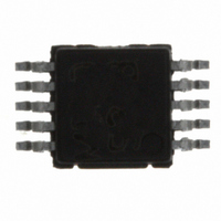
LM3354MM-4.1/NOPB National Semiconductor, LM3354MM-4.1/NOPB Datasheet - Page 8

LM3354MM-4.1/NOPB
Manufacturer Part Number
LM3354MM-4.1/NOPB
Description
IC CONVERTER DC/DC 90MA 10-MSOP
Manufacturer
National Semiconductor
Type
Step-Down (Buck), Step-Up (Boost), Switched Capacitor (Charge Pump)r
Datasheet
1.LM3354MM-4.1NOPB.pdf
(12 pages)
Specifications of LM3354MM-4.1/NOPB
Internal Switch(s)
Yes
Synchronous Rectifier
No
Number Of Outputs
1
Voltage - Output
4.1V
Current - Output
90mA
Frequency - Switching
1MHz
Voltage - Input
2.5 ~ 5.5 V
Operating Temperature
-40°C ~ 85°C
Mounting Type
Surface Mount
Package / Case
10-MSOP, Micro10™, 10-uMAX, 10-uSOP
For Use With
LM3354-4.1EVAL - BOARD EVALUATION LM3354-4.1
Lead Free Status / RoHS Status
Lead free / RoHS Compliant
Power - Output
-
Other names
LM3354MM-4.1
LM3354MM-4.1TR
LM3354MM-4.1TR
www.national.com
Applications Information
Operating Principle
The LM3354 is designed to provide a step-up/step-down
voltage regulation in battery powered systems. It combines
switched capacitor circuitry, reference, comparator, and
shutdown logic in a single 10-pin MSOP package. The
LM3354 can provide a regulated voltage between 1.8V and
5.0V from an input voltage between 2.5V and 5.5V. It can
supply a load current up to 90 mA (refer to Electrical Char-
acteristics).
As shown in Figure 1, the LM3354 employs two feedback
loops to provide regulation in the most efficient manner
possible. The first loop is from V
COMP, the AND gate G
switch array. The comparator’s output is high when V
less than the reference V
gating the clock to the switch array. In this manner, charge is
transferred to the output only when needed. The second
loop controls the gain configuration of the switch array. This
loop consists of the comparator, the digital control block, the
phase generator, and the switch array. The digital control
block computes the most efficient gain from a set of five
gains based on inputs from the A/D and the comparator. The
gain signal is sent to the phase generator which then sends
the appropriate timing and configuration signals to the switch
array. This dual loop provides regulation over a wide range of
loads efficiently.
Since efficiency is automatically optimized, the curves for
V
mance Characteristics section exhibit small variations. The
reason is that as input voltage or output load changes, the
digital control loops are making decisions on how to optimize
efficiency. As the switch array is reconfigured, small varia-
tions in output voltage and efficiency result. In all cases
where these small variations are observed, the part is oper-
ating correctly; minimizing output voltage changes and opti-
mizing efficiency.
OUT
vs. V
IN
and Efficiency vs. V
1
, the phase generator, and the
REF
. Regulation is provided by
OUT
IN
through the comparator
in the Typical Perfor-
FIGURE 1. Block Diagram
OUT
is
8
Charge Pump Capacitor Selection
A 0.33 µF ceramic capacitor is suggested for C1 and C2. To
ensure proper operation over temperature variations, an
X7R dielectric material is recommended.
Filter Capacitor Selection
a) CAPACITOR TECHNOLOGIES
The three major technologies of capacitors that can be used
as filter capacitors for LM3354 are: i) tantalum, ii) ceramic
and iii) polymer electrolytic technologies.
i) Tantalum
Tantalum capacitors are widely used in switching regulators.
Tantalum capacitors have the highest CV rating of any tech-
nology; as a result, high values of capacitance can be ob-
tained in relatively small package sizes. It is also possible to
obtain high value tantalum capacitors in very low profile
(
for low-profile, small size applications. Tantalums also pos-
sess very good temperature stability; i.e., the change in the
capacitance value, and impedance over temperature is rela-
tively small. However, the tantalum capacitors have relatively
high ESR values which can lead to higher voltage ripple and
their frequency stability (variation over frequency) is not very
good, especially at high frequencies (
ii) Ceramic
Ceramic capacitors have the lowest ESR of the three tech-
nologies and their frequency stability is exceptionally good.
These characteristics make the ceramics an attractive
choice for low ripple, high frequency applications. However,
the temperature stability of the ceramics is bad, except for
the X7R and X5R dielectric types. High capacitance values
(
yuden which are suitable for use with regulators. Ceramics
are taller and larger than the tantalums of the same capaci-
tance value.
<
>
1.2 mm) packages. This makes the tantalums attractive
1 µF) are achievable from companies such as Taiyo-
20018803
>
1 MHz).


