MAX8655ETN+ Maxim Integrated Products, MAX8655ETN+ Datasheet - Page 2
MAX8655ETN+
Manufacturer Part Number
MAX8655ETN+
Description
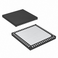
IC STEP-DN REG 25A 56-TQFN-EP
Manufacturer
Maxim Integrated Products
Type
Step-Down (Buck)r
Datasheets
1.MAX8655ETN.pdf
(24 pages)
2.MAX8655ETN.pdf
(23 pages)
3.MAX8655ETN.pdf
(24 pages)
4.MAX8655ETN.pdf
(24 pages)
Specifications of MAX8655ETN+
Internal Switch(s)
Yes
Synchronous Rectifier
No
Number Of Outputs
1
Voltage - Output
0.7 ~ 5.5 V
Current - Output
25A
Frequency - Switching
200kHz ~ 1MHz
Voltage - Input
4.5 ~ 25 V
Operating Temperature
-40°C ~ 85°C
Mounting Type
Surface Mount
Package / Case
56-TQFN Exposed Pad
Lead Free Status / RoHS Status
Lead free / RoHS Compliant
Power - Output
-
Lead Free Status / Rohs Status
Lead free / RoHS Compliant


ABSOLUTE MAXIMUM RATINGS
PVIN, IN, EN to GND ..............................................-0.3V to +30V
BST to LXB ............................................................-0.3V to +7.5V
LX, LXB to GND............ (-2.5V for < 50ns transient) -1V to +30V
ILIM2, ILIM1, SYNCO, FSYNC, OVP,
VL to PGND ...........................................................-0.3V to +7.5V
AVL, FB, POK, COMP, SS, MODE, REFIN to GND ..-0.3V to +6V
CS+, CS- to GND ....................................................-0.3V to +6V
PGND to GND to VLGND ......................................-0.3V to +0.3V
Highly Integrated, 25A, Wide-Input,
Internal MOSFET, Step-Down Regulator
Note 1: Package thermal resistances were obtained using the method described in JEDEC specification JESD51-7, using a four-
Stresses beyond those listed under “Absolute Maximum Ratings” may cause permanent damage to the device. These are stress ratings only, and functional
operation of the device at these or any other conditions beyond those indicated in the operational sections of the specifications is not implied. Exposure to
absolute maximum rating conditions for extended periods may affect device reliability.
ELECTRICAL CHARACTERISTICS
(V
Dual Mode is a trademark of Maxim Integrated Products, Inc.
2
PVIN Operating Voltage Range
IN Operating Voltage Range
IN Quiescent Supply Current
Shutdown Supply Current
PVIN Shutdown Supply Current
AVL Undervoltage-Lockout
Threshold
Output-Voltage Adjust Range
VL Regulation Voltage
AVL Regulation Voltage
AVL Output Current
SOFT-START
SS Shutdown Resistance
SS Soft-Start Current
REFIN INPUT
REFIN Dual Mode™ Threshold
REFIN Input Bias Current
REFIN Input Voltage Range
SCOMP to GND .....................................-0.3V to (V
IN
_______________________________________________________________________________________
= 12V, V
layer board. For detailed information on package thermal considerations, refer to www.maxim-ic.com/thermal-tutorial.
PARAMETER
BST
- V
LX
= 6.5V, T
A
= -40°C to +85°C, circuit of Figure 4, typical values are at T
VL = IN for V
V
EN = GND, V
I
V
V
Minimum output voltage is limited by minimum duty cycle
and external components
7V < V
5.5V < V
From SS to GND, V
V
V
IN
FB
PVIN
AVL
REF
REFIN
+ I
= 0.75V, no switching
rising, 3% typical hysteresis
= 0.625V
VL
= V
IN
= 0.7V to 1.5V
VL
+ I
< 28V
LX
AVL
< 7V, 1mA < I
= V
IN
IN
, EN = GND, V
< 7V
AVL
≤ 28V
BST
EN
+ 0.3V)
CONDITIONS
= 0V
LOAD
AVL
< 10mA
Operating Junction Temperature Range .......... -40°C to +125°C
Junction Temperature ......................................................+150°C
θ
θ
I
Storage Temperature Range .............................-65°C to +150°C
Lead Temperature (soldering, 10s) .................................+300°C
= V
LX (RMS)
JC
JT
junction to exposed pad) (Note 1) ...............................3.5°C/W
(thermal resistance from junction to the top) ............3.9°C/W
VL
(thermal resistance from
= V
.................................................................................27A
IN
= 5V
A
= +25°C, unless otherwise noted.) (Note 2)
V
4.900
3.90
1.0V
-250
MIN
AVL
4.5
0.7
6.0
10
18
3
0
-
4.975
TYP
4.15
6.5
20
23
2
1
5.050
+250
MAX
V
25.0
4.40
100
5.5
7.0
1.5
25
10
32
28
AVL
3
UNITS
mA
mA
µA
µA
µA
nA
Ω
V
V
V
V
V
V
V
V
Related parts for MAX8655ETN+
Image
Part Number
Description
Manufacturer
Datasheet
Request
R

Part Number:
Description:
MAX7528KCWPMaxim Integrated Products [CMOS Dual 8-Bit Buffered Multiplying DACs]
Manufacturer:
Maxim Integrated Products
Datasheet:
Part Number:
Description:
Single +5V, fully integrated, 1.25Gbps laser diode driver.
Manufacturer:
Maxim Integrated Products
Datasheet:
Part Number:
Description:
Single +5V, fully integrated, 155Mbps laser diode driver.
Manufacturer:
Maxim Integrated Products
Datasheet:
Part Number:
Description:
VRD11/VRD10, K8 Rev F 2/3/4-Phase PWM Controllers with Integrated Dual MOSFET Drivers
Manufacturer:
Maxim Integrated Products
Datasheet:
Part Number:
Description:
Highly Integrated Level 2 SMBus Battery Chargers
Manufacturer:
Maxim Integrated Products
Datasheet:
Part Number:
Description:
Current Monitor and Accumulator with Integrated Sense Resistor; ; Temperature Range: -40°C to +85°C
Manufacturer:
Maxim Integrated Products
Part Number:
Description:
TSSOP 14/A�/RS-485 Transceivers with Integrated 100O/120O Termination Resis
Manufacturer:
Maxim Integrated Products
Part Number:
Description:
TSSOP 14/A�/RS-485 Transceivers with Integrated 100O/120O Termination Resis
Manufacturer:
Maxim Integrated Products
Part Number:
Description:
QFN 16/A�/AC-DC and DC-DC Peak-Current-Mode Converters with Integrated Step
Manufacturer:
Maxim Integrated Products
Part Number:
Description:
TDFN/A/65V, 1A, 600KHZ, SYNCHRONOUS STEP-DOWN REGULATOR WITH INTEGRATED SWI
Manufacturer:
Maxim Integrated Products
Part Number:
Description:
Integrated Temperature Controller f
Manufacturer:
Maxim Integrated Products
Part Number:
Description:
SOT23-6/I�/45MHz to 650MHz, Integrated IF VCOs with Differential Output
Manufacturer:
Maxim Integrated Products
Part Number:
Description:
SOT23-6/I�/45MHz to 650MHz, Integrated IF VCOs with Differential Output
Manufacturer:
Maxim Integrated Products
Part Number:
Description:
EVALUATION KIT/2.4GHZ TO 2.5GHZ 802.11G/B RF TRANSCEIVER WITH INTEGRATED PA
Manufacturer:
Maxim Integrated Products
Part Number:
Description:
QFN/E/DUAL PCIE/SATA HIGH SPEED SWITCH WITH INTEGRATED BIAS RESISTOR
Manufacturer:
Maxim Integrated Products
Datasheet: