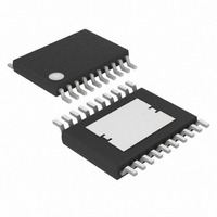
MAX5097BAUP+ Maxim Integrated Products, MAX5097BAUP+ Datasheet - Page 15

MAX5097BAUP+
Manufacturer Part Number
MAX5097BAUP+
Description
IC DC-DC CONV BUCK 20TSSOP
Manufacturer
Maxim Integrated Products
Type
Step-Down (Buck)r
Datasheet
1.MAX5097AATE.pdf
(21 pages)
Specifications of MAX5097BAUP+
Internal Switch(s)
Yes
Synchronous Rectifier
No
Number Of Outputs
2
Voltage - Output
5V, 1.24 ~ 11 V
Current - Output
600mA
Frequency - Switching
330kHz
Voltage - Input
5 ~ 40 V
Operating Temperature
-40°C ~ 125°C
Mounting Type
Surface Mount
Package / Case
20-TSSOP Exposed Pad, 20-eTSSOP, 20-HTSSOP
Power - Output
1.74W
Lead Free Status / RoHS Status
Lead free / RoHS Compliant
ripple is mainly composed of ΔV
capacitor discharge) and ΔV
age drop across the ESR of the output capacitor).
Normally, a good approximation of the output voltage
ripple is ΔV
capacitors, assume the contribution to the output volt-
age ripple from the ESR and the capacitor discharge to
be equal to 20% and 80%, respectively. If using alu-
minum electrolyte capacitors, assume the contribution
to the output voltage ripple from the ESR and the
capacitor discharge to be equal to 90% and 10%,
respectively.
Use the following equations for calculating the output
capacitance and its ESR for required peak-to-peak out-
put voltage ripple.
ΔI
the converter’s switching frequency.
The allowable deviation of the output voltage during
fast load transients also determines the output capaci-
tance, its ESR, and its equivalent series inductance
(ESL). The output capacitor supplies the load current
during a load step until the controller responds with a
greater duty cycle. The response time (t
depends on the closed-loop bandwidth of the converter
(see the Compensation Network section). The resistive
drop across the output capacitor’s ESR, the drop
across the capacitor’s ESL, and the capacitor dis-
charge, causes a voltage drop during the load step.
Use a combination of low-ESR tantalum/aluminum elec-
trolytic and ceramic capacitors for better transient load
and voltage ripple performance. Non-leaded capaci-
tors and/or multiple parallel capacitors help reduce the
ESL. Keep the maximum output voltage deviation
below the tolerable limits of the electronics being pow-
ered. Use the following equations to calculate the
required ESR, ESL, and capacitance value during a
load step:
P-P
is the peak-to-peak inductor current and f
RIPPLE
ESR
ESL
C
Quiescent-Current Linear Regulator Mode
OUT
C
OUT
=
=
______________________________________________________________________________________
40V, 600mA Buck Converters with Low-
≈ ΔV
ESR
=
Δ
Δ
Δ
V
I
V
I
STEP
STEP
ESL
=
ESR
I
16
=
STEP
ESR
Δ
×
Δ
×
×
V
t
I
P P
Δ
Δ
STEP
ESR
Δ
t
ESR
+ ΔV
RESPONSE
−
I
V
V
P P
Q
Q
−
×
(caused by the volt-
Q
f
SW
Q
. If using ceramic
(caused by the
RESPONSE
SW
is
)
where I
load step, and t
controller. The response time of the converter is
approximately one third of the inverse of its closed-loop
bandwidth and also depends on the phase margin.
The MAX5096/MAX5097 require an external Schottky/
fast-recovery diode rectifier as a freewheeling diode.
Connect this rectifier close to the device using short
leads and short PC board traces. Choose a rectifier
with a continuous current rating greater than the high-
est output current-limit threshold (1.9A) and with a volt-
age rating greater than the maximum expected input
voltage, V
rectifier to limit the negative voltage at LX. Avoid higher
than necessary reverse-voltage Schottky rectifiers that
have higher forward-voltage drops. Use a 60V (max)
Schottky rectifier with a 2A current rating. The Schottky
rectifier leakage current at high temperature significant-
ly increases the quiescent current in LDO Mode. In
applications where LDO Mode quiescent current is
important, use an ultra-fast switching diode to limit the
leakage current. In this type of application, use
MURS105, MURS120 for their fast-switching and low-
leakage features.
The discontinuous input current of the buck converter
causes large input ripple currents and therefore, the
input capacitor must be carefully chosen to keep the
input voltage ripple within design requirements. The
input voltage ripple is comprised of ΔV
the capacitor discharge) and ΔV
ESR of the input capacitor). The total voltage ripple is
the sum of ΔV
tance and ESR required for a specified ripple using the
following equations (continuous mode):
I
duty cycle.
where
OUT_MAX
STEP
IN
is the maximum output current and D is the
ESR
C
D
Δ
. Use a low forward-voltage-drop Schottky
is the load step, t
I
IN
P P
=
Q
−
V
=
and ΔV
=
RESPONSE
OUT
V
I
=
IN
⎛
⎜
⎝
OUT MAX
I
OUT MAX
(
V
IN
_
Input Capacitor Selection
Δ
ESR
V
_
V
−
IN
Q
Δ
V
V
OUT
×
×
. Calculate the input capaci-
ESR
is the response time of the
×
f
f
SW
SW
STEP
+
D
)
(
Rectifier Selection
Δ
1
×
×
I
−
P P
V
2
L
D
−
ESR
OUT
is the rise time of the
)
⎞
⎟
⎠
(caused by the
and
Q
(caused by
15


