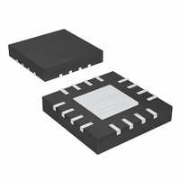
MAX5089ATE+T Maxim Integrated Products, MAX5089ATE+T Datasheet - Page 15

MAX5089ATE+T
Manufacturer Part Number
MAX5089ATE+T
Description
IC DC-DC CONV BUCK 16TQFN
Manufacturer
Maxim Integrated Products
Type
Step-Down (Buck)r
Datasheet
1.MAX5089ATE.pdf
(24 pages)
Specifications of MAX5089ATE+T
Internal Switch(s)
Yes
Synchronous Rectifier
Yes
Number Of Outputs
1
Voltage - Output
0.6 ~ 20 V
Current - Output
2A
Frequency - Switching
200kHz ~ 2.2MHz
Voltage - Input
4.5 ~ 23 V
Operating Temperature
-40°C ~ 125°C
Mounting Type
Surface Mount
Package / Case
16-TQFN Exposed Pad
Power - Output
2.67W
Lead Free Status / RoHS Status
Lead free / RoHS Compliant
The input ripple comprises mainly of ∆V
capacitor discharge) and ∆V
the input capacitor). The total voltage ripple is the sum of
∆V
the ESR and the capacitor discharge is equal to 50%
each. The following equations show the ESR and capaci-
tor requirement for a target voltage ripple at the input:
where
where I
and f
input capacitance at lower input voltages to avoid pos-
sible undershoot below the UVLO threshold during
transient loading.
The allowable output voltage ripple and the maximum
deviation of the output voltage during step load cur-
rents determine the output capacitance and its ESR.
The output ripple comprises of ∆V
capacitor discharge) and ∆V
the output capacitor). Use low-ESR ceramic or alu-
minum electrolytic capacitors at the output. For alu-
minum electrolytic capacitors, the entire output ripple is
contributed by ∆V
culate the ESR requirement and choose the capacitor
accordingly. If using ceramic capacitors, assume the
contribution to the output ripple voltage from the ESR
and the capacitor discharge to be equal. The following
equations show the output capacitance and ESR
requirement for a specified output voltage ripple.
Q
and ∆V
SW
OUT
D
∆I
is the switching frequency. Use additional
P P
=
ESR
is the output current, D is the duty cycle,
−
V
OUT
V
IN
=
ESR
C
. Assume the input voltage ripple from
ESR
C
IN
(
ESR
______________________________________________________________________________________
V
OUT
IN
=
=
V
=
. Use the ESR
I
−
IN
OUT
=
I
∆
V
∆
OUT
∆
OUT
V
×
8
V
I
ESR
P-P
f
Q
×
∆
SW
×
2.2MHz, 2A Buck Converters with an
∆
V
D
×
ESR
+
ESR
)
∆
ESR
V
×
f
(
∆
I
SW
×
1
Q
P-P
V
I
−
L
P P
OUT
2
×
(caused by the ESR of
(caused by the ESR of
D
−
f
SW
)
OUT
Output Capacitors
Q
and
Q
(caused by the
equation to cal-
(caused by the
Integrated High-Side Switch
where:
∆I
above and f
frequency.
The allowable deviation of the output voltage during
fast transient loads also determines the output capaci-
tance and its ESR. The output capacitor supplies the
step load current until the controller responds with a
greater duty cycle. The response time (t
depends on the closed-loop bandwidth of the convert-
er. The high switching frequency of MAX5088/
MAX5089 allows for a higher closed-loop bandwidth,
thus reducing t
requirement. The resistive drop across the output
capacitor’s ESR and the capacitor discharge causes a
voltage droop during a step load. Use a combination of
low-ESR tantalum and ceramic capacitors for better
transient load and ripple/noise performance. Keep the
maximum output voltage deviation below the tolerable
limits of the electronics being powered. When using a
ceramic capacitor, assume an 80% and 20% contribu-
tion from the output capacitance discharge and the
ESR drop, respectively. Use the following equations to
calculate the required ESR and capacitance value:
where I
response time of the controller. The controller response
time depends on the control-loop bandwidth.
The MAX5088/MAX5089 are available in thermally
enhanced 16-pin, 5mm x 5mm TQFN packages that
dissipate up to 2.7W at T
perature reaches +170°C, the MAX5088/MAX5089 shut
down (see the Thermal-Overload Protection section).
The power dissipated in the device is the sum of the
power dissipated from supply current (P
sipated due to switching the internal power MOSFET
(P
P-P
SW
), and the power dissipated due to the RMS cur-
is the peak-to-peak inductor current as calculated
STEP
SW
V
∆
is the load step and t
C
OUT RIPPLE
I
P P
RESPONSE
OUT
is the individual converter’s switching
−
_
ESR
=
=
(
V
I
OUT
STEP
IN
A
V
−
IN
and the output capacitance
= +70°C. When the die tem-
≅
V
=
×
OUT
×
∆
∆
∆
t
V
I
f
RESPONSE
STEP
SW
V
V
ESR
Power Dissipation
Q
ESR
)
×
×
V
+
L
OUT
RESPONSE
∆
V
Q
Q
), power dis-
RESPONSE
is the
15
)


