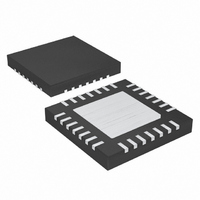
MAX5073ATI+T Maxim Integrated Products, MAX5073ATI+T Datasheet - Page 9

MAX5073ATI+T
Manufacturer Part Number
MAX5073ATI+T
Description
IC CONV BUCK/BOOST 28-TQFN
Manufacturer
Maxim Integrated Products
Type
Step-Down (Buck), Step-Up (Boost)r
Datasheet
1.MAX5073ETI.pdf
(25 pages)
Specifications of MAX5073ATI+T
Internal Switch(s)
Yes
Synchronous Rectifier
No
Number Of Outputs
2
Voltage - Output
0.8 ~ 28 V
Current - Output
1A, 2A
Frequency - Switching
200kHz ~ 2.2MHz
Voltage - Input
4.5 ~ 23 V
Operating Temperature
-40°C ~ 85°C
Mounting Type
Surface Mount
Package / Case
28-TQFN Exposed Pad
Power - Output
2.76W
Lead Free Status / RoHS Status
Lead free / RoHS Compliant
12, 13
18, 19
23, 24
27, 28
PIN
EP
10
11
14
15
16
17
20
21
22
25
26
2.2MHz, Dual-Output Buck or Boost Converter
BST1/VDD1
SOURCE1
SOURCE2
PGOOD1
PGOOD2
BYPASS
DRAIN1
COMP1
NAME
SGND
PGND
SGND
OSC
FB1
EN1
V+
VL
_______________________________________________________________________________________
Oscillator Frequency Set Input. Connect a resistor from OSC to SGND (R
frequency (see the Oscillator section). Set R
input frequency when using external synchronization (0.2f
when an external clock is connected to the SYNC input.
Input Supply Voltage. V+ voltage range from 5.5V to 23V. Connect the V+ and VL together for 4.5V to
5.5V input operation. Bypass with a minimum 0.1µF ceramic capacitor to SGND.
Internal 5.2V Linear Regulator Output. Use VL to drive the high-side switch at BST1/VDD1 and
BST2/VDD2. Bypass VL with a 0.1µF capacitor to PGND and a 4.7µF ceramic capacitor to SGND.
2.0V Output. Bypass to SGND with a 0.22µF or greater ceramic capacitor.
Compensation Connection for Converter 1 (See the Compensation Section)
Feed b ack Inp ut for C onver ter 1. C onnect FB1 to a r esi sti ve d i vi d er b etw een conver ter 1’ s outp ut and S GN D
to p r og r am the outp ut vol tag e. To set the outp ut vol tag e b el ow 0.8V , connect FB1 to a r esi sti ve vol tag e-
d i vi d er fr om BY P AS S to r eg ul ator 1’ s outp ut ( Fi g ur e 5) . S ee the S etti ng the O utp ut V ol tag e secti on.
Acti ve- H i g h E nab l e Inp ut for C onver ter 1. D r i ve E N 1 l ow to shut d ow n conver ter 1, d r i ve E N 1 hi g h for nor m al
op er ati on. U se E N 1 i n conj uncti on w i th E N 2 for sup p l y seq uenci ng . C onnect to V L for al w ays- on op er ati on.
Connection to the Converter 1 Internal MOSFET Drain.
Buck conver ter op er ati on— use the M OS FE T as a hi g h- si d e sw i tch and connect D RAIN 1 to the i np ut sup p l y.
Boost converter operation—use the MOSFET as a low-side switch and connect DRAIN1 to the inductor
and diode junction.
Buck Converter Operation—Bootstrap Flying-Capacitor Connection for Converter 1. Connect BST1/VDD1
to an external ceramic capacitor and diode according to the Standard Application Circuit (Figure 1).
Boost Converter Operation—Driver Bypass Capacitor Connection. Connect a low-ESR 0.1µF ceramic
capacitor from BST1/VDD1 to PGND.
Converter 1 Power-Good Output. Open-drain output goes low when converter 1’s output falls below
92.5% of its set regulation voltage. Use PGOOD1, PGOOD2, EN1, and EN2 to sequence the converters.
Converter 2 Power-Good Output. Open-drain output goes low when converter 2’s output falls below
92.5% of its set regulation voltage.
Connection to the Converter 1 Internal MOSFET Source.
Buck converter operation—connect SOURCE1 to the switched side of the inductor as shown in Figure 1.
Boost converter operation—connect SOURCE1 to PGND.
S i g nal G r ound . C onnect S G N D to the exp osed p ad . C onnect S G N D and P G N D tog ether at a si ng l e p oi nt.
Power Ground. Connect rectifier diode anode, input capacitor negative, output capacitor negative, and
VL bypass capacitor returns to PGND.
Connection to the Converter 2 Internal MOSFET Source.
Buck converter operation—connect SOURCE2 to the switched side of the inductor as shown in Figure 1.
Boost converter operation—connect SOURCE2 to PGND (Figure 8).
Exposed Paddle. Connect to SGND. Solder EP to the SGND plane for better thermal performance.
with Internal Power MOSFETs
OSC
FUNCTION
for equal to or lower oscillator frequency than the SYNC
Pin Description (continued)
SYNC
< f
OSC
< 1.2f
OSC
) to set the switching
SYNC
). R
OSC
is still required
9


