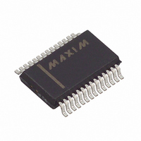
MAX1631EAI+T Maxim Integrated Products, MAX1631EAI+T Datasheet - Page 19

MAX1631EAI+T
Manufacturer Part Number
MAX1631EAI+T
Description
IC PS CTRLR FOR NOTEBOOKS 28SSOP
Manufacturer
Maxim Integrated Products
Type
Step-Down (Buck)r
Datasheet
1.MAX1634CAI.pdf
(29 pages)
Specifications of MAX1631EAI+T
Internal Switch(s)
No
Synchronous Rectifier
Yes
Number Of Outputs
2
Voltage - Output
3.3V, 5V, Adj
Current - Output
4A
Frequency - Switching
200kHz, 300kHz
Voltage - Input
4.2 ~ 30 V
Operating Temperature
-40°C ~ 85°C
Mounting Type
Surface Mount
Package / Case
28-SSOP
Power - Output
762mW
Output Voltage
2.5 V to 5.5 V, 3.3 V, 5 V
Input Voltage
4.2 V to 30 V
Mounting Style
SMD/SMT
Maximum Operating Temperature
+ 85 C
Minimum Operating Temperature
- 40 C
Lead Free Status / RoHS Status
Lead free / RoHS Compliant
The current-sense resistor value is calculated according
to the worst-case-low current-limit threshold voltage
(from the Electrical Characteristics table) and the peak
inductor current:
Use I
Value section
Use the calculated value of R
switches and specify inductor saturation-current ratings
according to the worst-case high-current-limit threshold
voltage:
Low-inductance resistors, such as surface-mount
metal-film, are recommended.
Connect low-ESR bulk capacitors and small ceramic
capacitors (0.1µF) directly to the drains on the high-
side MOSFETs. The bulk input filter capacitor is usually
selected according to input ripple current requirements
and voltage rating, rather than capacitor value.
Electrolytic capacitors with low enough effective series
resistance (ESR) to meet the ripple current requirement
invariably have sufficient capacitance values.
Aluminum electrolytic capacitors, such as Sanyo
OS-CON or Nichicon PL, are superior to tantalum
types, which carry the risk of power-up surge-current
failure, especially when connecting to robust AC
adapters or low-impedance batteries. RMS input ripple
current (I
load current, with the worst case occurring at V
V
Bypass the V+ input with a 4.7µF tantalum capacitor
paralleled with a 0.1µF ceramic capacitor, close to the
IC. A 10Ω series resistor to V
Therefore, when V
OUT
:
PEAK
RMS
I
I
RMS
RMS
from the second equation in the Inductor
) is determined by the input voltage and
I
= I
=
PEAK(MAX)
Current-Sense Resistor Value
R
______________________________________________________________________________________
IN
LOAD
I
LOAD
SENSE
is 2 x V
2
Multi-Output, Low-Noise Power-Supply
x
=
Input Capacitor Value
=
OUT
Controllers for Notebook Computers
V
IN
SENSE
OUT
I
80mV
PEAK
R
is also recommended.
120mV
SENSE
:
(V - V
V
IN
IN
to size the MOSFET
Bypassing V+
OUT
)
IN
= 2 x
Bypass the VL output with a 4.7µF tantalum capacitor
paralleled with a 0.1µF ceramic capacitor, close to the
device.
The output filter capacitor values are generally deter-
mined by the ESR and voltage rating requirements, rather
than actual capacitance requirements for loop stability. In
other words, the low-ESR electrolytic capacitor that meets
the ESR requirement usually has more output capaci-
tance than is required for AC stability. Use only special-
ized low-ESR capacitors intended for switching-regulator
applications, such as AVX TPS, Sprague 595D, Sanyo
OS-CON, or Nichicon PL series. To ensure stability, the
capacitor must meet both minimum capacitance and
maximum ESR values as given in the following equations:
These equations are worst case, with 45 degrees of
phase margin to ensure jitter-free, fixed-frequency
operation and provide a nicely damped output
response for zero to full-load step changes. Some cost-
conscious designers may wish to bend these rules with
less-expensive capacitors, particularly if the load lacks
large step changes. This practice is tolerable if some
bench testing over temperature is done to verify
acceptable noise and transient response.
No well-defined boundary exists between stable and
unstable operation. As phase margin is reduced, the
first symptom is a bit of timing jitter, which shows up as
blurred edges in the switching waveforms where the
scope won’t quite sync up. Technically speaking, this
jitter (usually harmless) is unstable operation, since the
duty factor varies slightly. As capacitors with higher
ESRs are used, the jitter becomes more pronounced,
and the load-transient output voltage waveform starts
looking ragged at the edges. Eventually, the load-tran-
sient waveform has enough ringing on it that the peak
noise levels exceed the allowable output voltage toler-
ance. Note that even with zero phase margin and gross
instability present, the output voltage noise never gets
much worse than I
Designers of RF communicators or other noise-sensi-
tive analog equipment should be conservative and stay
within the guidelines. Designers of notebook computers
and similar commercial-temperature-range digital
(can be multiplied by 1.5; see text below)
C
R
ESR
OUT
<
>
Output Filter Capacitor Value
PEAK
R
V
SENSE
REF
V
x R
(1 + V
OUT
V
REF
ESR
x V
x R
OUT
(under constant loads).
OUT
SENSE
/ V
IN(MIN)
Bypassing VL
x f
)
19


