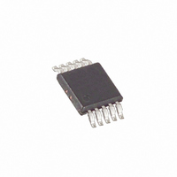
MAX1846EUB+ Maxim Integrated Products, MAX1846EUB+ Datasheet - Page 11

MAX1846EUB+
Manufacturer Part Number
MAX1846EUB+
Description
IC CNTRLR PWM HI EFF 10-UMAX
Manufacturer
Maxim Integrated Products
Type
Inverting, Flybackr
Datasheet
1.MAX1847EEE.pdf
(20 pages)
Specifications of MAX1846EUB+
Internal Switch(s)
No
Synchronous Rectifier
No
Number Of Outputs
1
Voltage - Output
-0.5 ~ -200 V
Current - Output
5A
Frequency - Switching
100kHz ~ 500kHz
Voltage - Input
3 ~ 16.5 V
Operating Temperature
-40°C ~ 85°C
Mounting Type
Surface Mount
Package / Case
10-MSOP, Micro10™, 10-uMAX, 10-uSOP
Power - Output
444mW
Duty Cycle (max)
97 %
Output Voltage
1.25 V
Mounting Style
SMD/SMT
Switching Frequency
500 KHz
Operating Supply Voltage
3 V to 16.5 V
Supply Current
0.75 mA
Maximum Operating Temperature
+ 85 C
Fall Time
200 ns
Minimum Operating Temperature
- 40 C
Output Power
444 mW
Rise Time
200 ns
Lead Free Status / RoHS Status
Lead free / RoHS Compliant
The MAX1846/MAX1847 current-mode PWM controllers
use an inverting topology that is ideal for generating
output voltages from -500mV to -200V. Features include
shutdown, adjustable internal operating frequency or
synchronization to an external clock, soft-start,
adjustable current limit, and a wide (+3V to +16.5V)
input range.
The architecture of the MAX1846/MAX1847 current-
mode PWM controller is a BiCMOS multi-input system
that simultaneously processes the output-error signal,
the current-sense signal, and a slope-compensation
ramp ( Functional Diagram ). Slope compensation pre-
vents subharmonic oscillation, a potential result in cur-
rent-mode regulators operating at greater than 50%
duty cycle. The controller uses fixed-frequency, cur-
rent-mode operation where the duty ratio is set by the
input-to-output voltage ratio. The current-mode feed-
back loop regulates peak inductor current as a function
of the output error signal.
The MAX1846/MAX1847 incorporate an internal low-
dropout regulator (LDO). This LDO has a 4.25V output
and powers all MAX1846/MAX1847 functions (exclud-
ing EXT) for the primary purpose of stabilizing the per-
formance of the IC over a wide input voltage range
(+3V to +16.5V). The input to this regulator is connect-
ed to IN, and the dropout voltage is typically 100mV, so
that when V
minus 100mV. When the LDO is in dropout, the
MAX1846/MAX1847 still operate with V
For best performance, it is recommended to connect
VL to IN when the input supply is less than 4.5V.
The MAX1846/MAX1847 have an undervoltage lockout
circuit that monitors the voltage at VL. If VL falls below
the UVLO threshold (2.8V typ), the control logic turns the
P-channel FET off (EXT high impedance). The rest of the
IC circuitry is still powered and operating. When VL
increases to 60mV above the UVLO threshold, the IC
resumes operation from a start up condition (soft-start).
The MAX1846/MAX1847 feature a “digital” soft-start
that is preset and requires no external capacitor. Upon
startup, the FB threshold decrements from the refer-
ence voltage to 0 in 64 steps over 1024 cycles of f
or f
a scope picture of the soft-start operation. Soft-start is
implemented: 1) when power is first applied to the IC,
SYNC
. See the Typical Operating Characteristics for
IN
is less than 4.35V, VL is typically V
______________________________________________________________________________________
Detailed Description
Undervoltage Lockout
Internal Regulator
PWM Controller
IN
as low as 3V.
High-Efficiency, Current-Mode,
Soft-Start
OSC
IN
Inverting PWM Controller
2) when exiting shutdown with power already applied,
and 3) when exiting undervoltage lockout.
The MAX1847 shuts down to reduce the supply current
to 10µA when SHDN is low. In this mode, the internal ref-
erence, error amplifier, comparators, and biasing circuit-
ry turn off. The EXT output becomes high impedance
and the external pullup resistor connected to EXT pulls
V
shutdown mode, the converter’s output goes to 0.
The MAX1847 is capable of synchronizing its switching
frequency with an external clock source. Drive SYNC
with a logic-level clock input signal to synchronize the
MAX1847. A switching cycle starts on the rising edge
of the signal applied to SYNC. Note that the frequency
of the signal applied to SYNC must be higher than the
default frequency set by R
required so that the internal clock does not start a
switching cycle prematurely. If SYNC is inactive for an
entire clock cycle of the internal oscillator, the internal
oscillator takes over the switching operation. Choose
R
The MAX1847 features an option to utilize an N-channel
MOSFET configuration, rather than the typical p-chan-
nel MOSFET configuration (Figure 1). In order to drive
the different polarities of these MOSFETs, the MAX1847
is capable of reversing the phase of EXT by 180
degrees. When driving a P-channel MOSFET, connect
POL to GND. When driving an n-channel MOSFET, con-
nect POL to VL. These POL connections ensure the
proper polarity for EXT. For design guidance in regard
to this application, refer to the MAX1856 data sheet.
In order to start the design procedure, a few parameters
must be identified: the minimum input voltage expected
(V
(V
expected maximum load current (I
This is a simple calculation used to shorten the verifica-
tion equations:
EXT
FREQ
IN(MAX)
IN(MIN)
to V
such that f
IN
), the desired output voltage (V
), the maximum input voltage expected
, turning off the P-channel MOSFET. When in
Calculate the Equivalent Load Resistance
R
OSC
LOAD
EXT Polarity (MAX1847 only)
Frequency Synchronization
Shutdown (MAX1847 only)
= 0.9
= V
Design Procedure
OUT
Initial Specifications
FREQ
f
SYNC
/ I
LOAD
LOAD
. This frequency is
(MAX1847 only)
.
).
OUT
), and the
11


