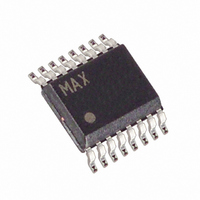
MAX1701EEE+ Maxim Integrated Products, MAX1701EEE+ Datasheet - Page 2

MAX1701EEE+
Manufacturer Part Number
MAX1701EEE+
Description
IC DC-DC CONV STP UP 1A 16-QSOP
Manufacturer
Maxim Integrated Products
Type
Step-Up (Boost)r
Datasheet
1.MAX1700EEE.pdf
(16 pages)
Specifications of MAX1701EEE+
Internal Switch(s)
Yes
Synchronous Rectifier
Yes
Number Of Outputs
1
Voltage - Output
2.2 ~ 5.5 V
Current - Output
800mA
Frequency - Switching
300kHz
Voltage - Input
0.7 ~ 5.5 V
Operating Temperature
-40°C ~ 85°C
Mounting Type
Surface Mount
Package / Case
16-QSOP
Power - Output
667mW
Lead Free Status / RoHS Status
Lead free / RoHS Compliant
ABSOLUTE MAXIMUM RATINGS
ONA, ONB, OUT, AO, POK, LBO to GND...................-0.3V, +6V
PGND to GND.....................................................................±0.3V
LX to PGND.....................................................-0.3V,V
CLK/SEL, AIN, REF, FB, LBP, LBN, POUT to GND............-0.3V,
V
Continuous Power Dissipation (T
ELECTRICAL CHARACTERISTICS
(CLK/SEL = ONA =
T
1-Cell to 3-Cell, High-Power (1A),
Low-Noise, Step-Up DC-DC Converters
Stresses beyond those listed under “Absolute Maximum Ratings” may cause permanent damage to the device. These are stress ratings only, and functional
operation of the device at these or any other conditions beyond those indicated in the operational sections of the specifications is not implied. Exposure to
absolute maximum rating conditions for extended periods may affect device reliability.
2
DC-DC CONVERTER
DC-DC SWITCHES
Input Voltage Range (Note 1)
Minimum Start-Up Voltage
(Note 2)
Frequency in Start-Up Mode
Output Voltage (Note 3)
FB Regulation Voltage
FB Input Current
Output Voltage Adjust Range
Output Voltage Lockout
Threshold
Load Regulation (Note 5)
Supply Current in Shutdown
Supply Current in Low-Power
Mode (Note 6)
Supply Current in Low-Noise
Mode (Note 6)
POUT Leakage Current
LX Leakage Current
Switch On-Resistance
N-Channel Current Limit
P-Channel Turn-Off Current
A
OUT
16-QSOP (Derate 8.30mW/°C above +70°C) ...............667mW
= 0°C to +85°C, unless otherwise noted. Typical values are at T
_______________________________________________________________________________________
+0.3V ...................................................................................
PARAMETER
ONB = FB = PGND = GND, OUT = POUT, V
A
=+70°C)
I
V
V
includes load regulation error for 0A ≤ I
Adjustable output, CLK/SEL = OUT, V
includes load regulation error for 0A ≤ I
V
(Note 4)
CLK/SEL = OUT, No load to full load
V
CLK/SEL = GND (MAX1700)
CLK/SEL = GND (MAX1701)
CLK/SEL = OUT (MAX1700)
CLK/SEL = OUT (MAX1701)
V
V
N-channel
P-channel
CLK/SEL = OUT
CLK/SEL = GND
CLK/SEL = GND
LOAD
OUT
FB
FB
LX
LX
ONB
< 0.1V, CLK/SEL = OUT, V
= 1.25V
= 0V, V
= V
= 1.5V
< 1mA, T
= 3.6V
ONB
OUT
= V
A
= 5.5V
OUT
POUT
= +25°C
= 5.5V
+0.3V
CONDITIONS
MAX1700
MAX1701
CLK/SEL = GND
CLK/SEL = OUT
A
BATT
OUT
= +25°C.)
Operating Temperature Ranges
Junction Temperature ......................................................+150°C
Storage Temperature Range .............................-65°C to +160°C
Lead Temperature (soldering, 10sec) .............................+300°C
MAX1700EEE, MAX1701EEE ...........................-40°C to +85°C
= 3.6V (Note 6); MAX1701: AIN = LBN = GND, LBP = REF,
= 2.4V,
BATT
LX
LX
≤ 0.55A
≤ 0.55A
= 2.4V,
1.210
1100
3.17
MIN
250
2.5
2.0
40
20
1300
TYP
3.30
1.24
0.01
2.15
0.13
0.25
-1.6
150
125
140
400
0.7
0.9
0.1
0.1
0.1
0.2
35
55
3
1.255
MAX
1600
3.38
0.45
0.28
300
110
250
300
550
120
5.5
1.1
5.5
2.3
0.5
20
20
20
70
20
20
UNITS
kHz
mA
mA
nA
µA
µA
µA
µA
µA
%
Ω
V
V
V
V
V
V


