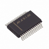
MAX786CAI+T Maxim Integrated Products, MAX786CAI+T Datasheet - Page 14

MAX786CAI+T
Manufacturer Part Number
MAX786CAI+T
Description
IC CNTRLR PWR SUP DL 28SSOP
Manufacturer
Maxim Integrated Products
Type
Step-Down (Buck)r
Datasheet
1.MAX786CAI.pdf
(20 pages)
Specifications of MAX786CAI+T
Internal Switch(s)
No
Synchronous Rectifier
Yes
Number Of Outputs
2
Voltage - Output
3.3V, 5V
Current - Output
3A
Frequency - Switching
200kHz, 300kHz
Voltage - Input
5.5 ~ 30 V
Operating Temperature
0°C ~ 70°C
Mounting Type
Surface Mount
Package / Case
28-SSOP
Power - Output
762mW
Output Voltage
3.3 V, 3.45 V, 3.6 V
Input Voltage
5.5 V to 30 V
Mounting Style
SMD/SMT
Maximum Operating Temperature
+ 70 C
Minimum Operating Temperature
0 C
Lead Free Status / RoHS Status
Lead free / RoHS Compliant
V
value should include the worst-case conditions under
which the power supply is expected to function, such
as no-load (standby) operation when a battery charger
is connected but no battery is installed. V
exceed 30V.
V
value should be taken at the full-load operating cur-
rent under the lowest battery conditions. If V
below about 6.5V, the filter capacitance required to
maintain good AC load regulation increases, and the
current limit for the +5V supply has to be increased
for the same load level.
Three inductor parameters are required: the inductance
value (L), the peak inductor current (I
coil resistance (R
where:
A higher value of LIR allows smaller inductance, but
results in higher losses and higher ripple.
The highest peak inductor current (I
load current (I
current (I
typically chosen as 30% of the maximum DC load cur-
rent, so the peak inductor current is 1.15 times I
The peak inductor current at full load is given by:
I
The coil resistance should be as low as possible,
preferably in the low milliohms. The coil is effectively in
series with the load at all times, so the wire losses alone
are approximately:
In general, select a standard inductor that meets the L,
I
standard inductor is unavailable, choose a core with an
LI
largest wire that will fit the core.
Dual-Output Power-Supply
Controller for Notebook Computers
14
LPEAK
LPEAK
IN(MAX)
IN(MIN)
2
parameter greater than (L) (I
______________________________________________________________________________________
, and R
= I
, the minimum input (battery) voltage. This
, the maximum input (battery) voltage. This
LPP
OUT
L = ————————————
V
V
f = switching frequency, normally 300kHz;
I
LIR = ratio of inductor peak-to-peak AC
current to average DC load current, typically 0.3.
Power loss = (I
OUT
OUT
IN(MAX)
). The peak-to-peak AC inductor current is
OUT
L
+ —————————————.
(V
(V
= maximum DC load current (A);
requirements (see Tables 1 and 2). If a
= output voltage (3.3V or 5V);
OUT
IN(MAX)
) plus half the peak-to-peak AC inductor
L
). The inductance is:
(V
= maximum input voltage (V);
) (V
OUT
(2) (f) (L) (V
) (f) (I
IN(MAX)
) (V
OUT
IN(MAX)
OUT
2
) (R
- V
) (LIR)
L
IN(MAX)
OUT
).
LPEAK
Inductor (L1, L2)
LPEAK
- V
)
OUT
LPEAK
2
)
) equals the DC
), and use the
IN(MAX)
)
), and the
OUT
IN(MIN)
cannot
.
is
The sense resistors must carry the peak current in the
inductor, which exceeds the full DC load current. The
internal current limiting starts when the voltage across
the sense resistors exceeds 100mV nominally, 80mV
minimum. Use the minimum value to ensure adequate
output current capability: For the +3.3V supply, R1 =
80mV / (1.15 x I
80mV/(1.15 x I
Since the sense resistance values (e.g., R1 = 25mΩ for
I
traces on a printed circuit board, trace resistance can
contribute significant errors. To prevent this, Kelvin con-
nect the CS_ and FB_ pins to the sense resistors; i.e.,
use separate traces not carrying any of the inductor or
load current, as shown in Figure 5.
Run these traces parallel at minimum spacing from one
another. The wiring layout for these traces is critical for
stable, low-ripple outputs (see the Layout and
Grounding section).
The four N-channel power MOSFETs are usually iden-
tical and must be “logic-level” FETs; that is, they must
be fully on (have low r
source drive voltage. The MOSFET r
ideally be about twice the value of the sense resistor.
MOSFETs with even lower r
capacitance, which increases switching time and
transition losses.
MOSFETs with low gate-threshold voltage specifica-
tions (i.e., maximum V
preferred, especially for high-current (5A) applications.
The output filter capacitors determine the loop stability
and output ripple voltage. To ensure stability, the mini-
mum capacitance and maximum ESR values are:
and,
where:
OUT
= 3A) are similar to a few centimeters of narrow
Output Filter Capacitors (C6, C7, C12)
C
ESR
C
V
V
R
GBWP = gain-bandwidth product, 60kHz;
ESR
REF
OUT
CS
F
F
Current-Sense Resistors (R1, R2)
= output filter capacitance (F);
> —————————————
CF
CF
= sense resistor (Ω);
OUT
= reference voltage, 3.3V;
= output voltage, 3.3V or 5V;
(V
< ——————
= output filter capacitor ESR (Ω).
OUT
), assuming that LIR = 0.3.
OUT
(V
MOSFET Switches (N1-N4)
) (R
OUT
GS(TH)
); for the +5V supply, R2 =
V
REF
CS
) (R
DS(ON)
V
) (2) (π) (GBWP)
REF
CS
DS(ON)
= 2V rather than 3V) are
)
) with only 4V gate-
have higher gate
DS(ON)
should


