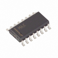
MAX1653ESE Maxim Integrated Products, MAX1653ESE Datasheet - Page 21

MAX1653ESE
Manufacturer Part Number
MAX1653ESE
Description
IC CTRLR DCDC PWM STPDWN 16-SOIC
Manufacturer
Maxim Integrated Products
Type
Step-Down (Buck)r
Datasheet
1.MAX1655ESE.pdf
(28 pages)
Specifications of MAX1653ESE
Internal Switch(s)
No
Synchronous Rectifier
Yes
Number Of Outputs
1
Voltage - Output
2.5 ~ 5.5 V
Current - Output
10A
Frequency - Switching
150kHz, 300kHz
Voltage - Input
4.5 ~ 30 V
Operating Temperature
-40°C ~ 85°C
Mounting Type
Surface Mount
Package / Case
16-SOIC (3.9mm Width)
Power - Output
696mW
Output Voltage
2.5 V to 5.5 V
Output Current
10 A
Input Voltage
4.5 V to 30 V
Mounting Style
SMD/SMT
Maximum Operating Temperature
+ 85 C
Minimum Operating Temperature
- 40 C
Lead Free Status / RoHS Status
Contains lead / RoHS non-compliant
Available stocks
Company
Part Number
Manufacturer
Quantity
Price
Company:
Part Number:
MAX1653ESE
Manufacturer:
MAXIM
Quantity:
126
Company:
Part Number:
MAX1653ESE
Manufacturer:
MAXIM
Quantity:
9
Part Number:
MAX1653ESE
Manufacturer:
MAXIM/美信
Quantity:
20 000
Company:
Part Number:
MAX1653ESE+
Manufacturer:
Maxim
Quantity:
50
Part Number:
MAX1653ESE+
Manufacturer:
MAXIM/美信
Quantity:
20 000
Company:
Part Number:
MAX1653ESE+T
Manufacturer:
MAXIM
Quantity:
7
Place a small ceramic capacitor (0.1µF) between V+ and
GND, close to the device. Also, connect a low-ESR bulk
capacitor directly to the drain of the high-side MOSFET.
Select the bulk input filter capacitor according to input
ripple-current requirements and voltage rating, rather
than capacitor value. Electrolytic capacitors that have
low enough effective series resistance (ESR) to meet the
ripple-current requirement invariably have more than
adequate capacitance values. Ceramic capacitors or
low-ESR aluminum-electrolytic capacitors such as Sanyo
OS-CON or Nichicon PL are preferred. Tantalum types
are also acceptable but may be less tolerant of high
input surge currents. RMS input ripple current is deter-
mined by the input voltage and load current, with the
worst possible case occurring at V
The output filter capacitor values are determined by the
ESR, capacitance, and voltage rating requirements.
Electrolytic and tantalum capacitors are generally cho-
sen by voltage rating and ESR specifications, as they
will generally have more output capacitance than is
required for AC stability. Use only specialized low-ESR
capacitors intended for switching-regulator applications,
such as AVX TPS, Sprague 595D, Sanyo OS-CON, or
Nichicon PL series. To ensure stability, the capacitor
must meet both minimum capacitance and maximum
ESR values as given in the following equations:
These equations are “worst-case” with 45 degrees of
phase margin to ensure jitter-free fixed-frequency opera-
tion and provide a nicely damped output response for
zero to full-load step changes. Some cost-conscious
designers may wish to bend these rules by using less
expensive (lower quality) capacitors, particularly if the
load lacks large step changes. This practice is tolerable if
some bench testing over temperature is done to verify
acceptable noise and transient response.
There is no well-defined boundary between stable and
unstable operation. As phase margin is reduced, the
(can be multiplied by 1.5, see note below)
I
I
RMS
RMS
C
OUT
R
> ––––––––––––––––———–––
ESR
I
I
LOAD
LOAD
Output Filter Capacitor Value
V
______________________________________________________________________________________
REF
< ————————
V
(1 + V
OUT
/
x
R
2
SENSE
V
Input Capacitor Value
when V
x R
V
REF
OUT VIN
OUT
SENSE
x V
IN
/ V
(
DC-DC Controllers in 16-Pin QSOP
IN
V
OUT
High-Efficiency, PWM, Step-Down
= 2 x V
IN
IN(MIN)
is
x f
VOUT
2
OUT
x V
)
)
OUT
:
first symptom is a bit of timing jitter, which shows up as
blurred edges in the switching waveforms where the
scope won’t quite sync up. Technically speaking, this
(usually) harmless jitter is unstable operation, since the
switching frequency is now nonconstant. As the capac-
itor quality is reduced, the jitter becomes more pro-
nounced and the load-transient output voltage
waveform starts looking ragged at the edges.
Eventually, the load-transient waveform has enough
ringing on it that the peak noise levels exceed the
allowable output voltage tolerance. Note that even with
zero phase margin and gross instability present, the
output voltage noise never gets much worse than I
x R
Note: Designers of RF communicators or other noise-
sensitive analog equipment should be conservative
and stick to the ESR guidelines. Designers of notebook
computers and similar commercial-temperature-range
digital systems can multiply the R
of 1.5 without hurting stability or transient response.
The output voltage ripple is usually dominated by the
ESR of the filter capacitor and can be approximated as
I
full equation for ripple in the continuous mode is
V
Idle Mode, the inductor current becomes discontinuous
with high peaks and widely spaced pulses, so the noise
can actually be higher at light load compared to full load.
In Idle Mode, the output ripple can be calculated as:
Buck-plus-flyback applications, sometimes called “cou-
pled-inductor” topologies, use a transformer to generate
multiple output voltages. The basic electrical design is a
simple task of calculating turns ratios and adding the
power delivered to the secondary in order to calculate the
current-sense resistor and primary inductance. However,
extremes of low input-output differentials, widely different
output loading levels, and high turns ratios can compli-
cate the design due to parasitic transformer parameters
such as interwinding capacitance, secondary resistance,
and leakage inductance. For examples of what is possi-
ble with real-world transformers, see the graphs of
Maximum Secondary Current vs. Input Voltage in the
Typical Operating Characteristics.
RIPPLE
NOISE(p-p)
ESR
———————————————————
(0.025)
(under constant loads, at least).
x R
ESR
V
= I
NOISE(p-p)
2
. There is also a capacitive term, so the
RIPPLE
x L x [1 / V
(R
SENSE
(MAX1652/MAX1654 Only)
x [R
= —————— +
OUT
ESR
)
0.025 x R
2
x C
R
Transformer Design
+ 1 / (V
+ 1 / (8 x f x C
SENSE
OUT
ESR
ESR
IN
value by a factor
- V
OUT
OUT
)]
PEAK
)]. In
21


