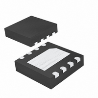
MAX15032ATA+T Maxim Integrated Products, MAX15032ATA+T Datasheet - Page 7

MAX15032ATA+T
Manufacturer Part Number
MAX15032ATA+T
Description
IC DC-DC CONV STEP-UP 8-TDFN
Manufacturer
Maxim Integrated Products
Type
Step-Up (Boost)r
Datasheet
1.MAX15032ATAT.pdf
(10 pages)
Specifications of MAX15032ATA+T
Internal Switch(s)
Yes
Synchronous Rectifier
No
Number Of Outputs
1
Voltage - Output
6.6 ~ 36 V
Current - Output
1A
Frequency - Switching
500kHz
Voltage - Input
2.7 ~ 11 V
Operating Temperature
-40°C ~ 125°C
Mounting Type
Surface Mount
Package / Case
8-TDFN Exposed Pad
Power - Output
1.95W
Lead Free Status / RoHS Status
Lead free / RoHS Compliant
The MAX15032 constant-frequency, current-mode,
pulse-width-modulating (PWM) boost converter is
intended for low-voltage systems that often need a
locally generated high voltage. This device is capable
of generating low-noise, high-output voltage required
for PIN and varactor diode biasing and LCD displays.
The MAX15032 operates either from +2.7V to +5.5V or
from +5.5V to +11V. For +2.7V to +5.5V operation, an
internal charge pump with an external 10nF ceramic
capacitor is used. The MAX15032 also features a shut-
down logic input to disable the device and reduce its
standby current to 0.5µA (max).
The MAX15032 operates in discontinuous mode in order
to reduce the switching noise caused by the reverse
recovery charge of the rectifier diode. Other continuous
mode boost converters generate large voltage spikes at
the output when the LX switch turns on because there is
a conduction path between the output, diode, and
switch to ground during the time needed for the diode to
turn off and reverse its bias voltage. To reduce the out-
put noise even further, the LX switch turns off by taking
6.8ns typically to transition from “ON” to “OFF.” As a
consequence, the positive slew rate of the LX node is
reduced and the current from the inductor does not
“force” the output voltage as hard as would be the case
if the LX switch were to turn off more quickly.
Also, the constant-frequency (500kHz) PWM architec-
ture generates an output voltage ripple that is easy to
filter. A 40V lateral DMOS device used as the internal
power switch makes the device ideal for boost convert-
ers with output voltages up to 36V.
The MAX15032 can also be used in other topologies
where the PWM switch is grounded, like SEPIC and
flyback.
The heart of the MAX15032 current-mode PWM con-
troller is a BiCMOS multi-input comparator that simulta-
neously processes the output-error signal and switch
current signal. The main PWM comparator is direct
summing, lacking a traditional error amplifier and its
associated phase shift. The direct summing configura-
_______________________________________________________________________________________
Detailed Description
500kHz, 36V Output, 600mW PWM
PWM Controller
Step-Up DC-DC Converter
tion approaches ideal cycle-by-cycle control over the
output voltage since there is no conventional error
amplifier in the feedback path.
The device operates in PWM mode using a fixed-fre-
quency, current-mode operation. The current-mode fre-
quency loop regulates the peak inductor current as a
function of the output error signal. The current-mode
PWM controller is intended for discontinuous conduc-
tion mode (DCM) operation. No internal slope compen-
sation is added to the current signal.
The MAX15032 features an active-low shutdown input
(SHDN). Pull SHDN low to enter shutdown. During shut-
down, the supply current drops to 0.5µA (max).
However, the output remains connected to the input
through the inductor and output rectifier, holding the
output voltage to one diode drop below V
MAX15032 shuts down. Connect SHDN to IN for
always-on operation.
At low supply voltages (+2.7V to +5.5V), an internal
charge-pump circuit and an external 10nF ceramic
capacitor double the available supply voltage in order
to drive the internal switch efficiently.
In the +5.5V to +11V supply voltage range, the charge
pump must be disabled by connecting CP to IN and
leaving CN unconnected.
Set the MAX15032 output voltage by connecting a
resistive divider from the output to FB to GND (see the
Typical Operating Circuit ). Select R2 (FB to GND resis-
tor) between 6kΩ and 10kΩ. Calculate R1 (V
resistor) with the following equation:
where V
table) and V
FB
= 1.245V (see the Electrical Characteristics
OUT
can range from (V
R
1
=
Setting the Output Voltage
R
2
⎡
⎢
⎢
⎣
⎛
⎜
⎝
V
Design Procedure
V
OUT
FB
Shutdown ( SHDN )
⎞
⎟
⎠
IN
−
1
⎤
⎥
⎥
⎦
+ 1V) to 36V.
Charge Pump
IN
OUT
when the
to FB
7


