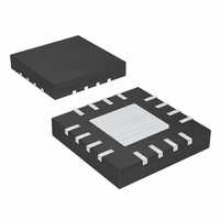
MAX5092BATE+T Maxim Integrated Products, MAX5092BATE+T Datasheet - Page 3

MAX5092BATE+T
Manufacturer Part Number
MAX5092BATE+T
Description
IC REG LDO W/BOOST 16TQFN
Manufacturer
Maxim Integrated Products
Type
Step-Up (Boost)r
Datasheet
1.MAX5092AATE.pdf
(24 pages)
Specifications of MAX5092BATE+T
Internal Switch(s)
Yes
Synchronous Rectifier
No
Number Of Outputs
2
Voltage - Output
5V, 1.5 ~ 9 V
Current - Output
250mA
Voltage - Input
3.5 ~ 72 V
Operating Temperature
-40°C ~ 125°C
Mounting Type
Surface Mount
Package / Case
16-TQFN Exposed Pad
Power - Output
2.67W
Polarity
Positive
Input Voltage Max
72 V
Output Voltage
1.5 V to 9 V, 5 V
Output Type
Adjustable, Fixed
Dropout Voltage (max)
1.6 V at 250 mA
Output Current
250 mA
Line Regulation
1.6 mV / V
Load Regulation
0.2 mV / mA
Voltage Regulation Accuracy
1.5 %
Maximum Power Dissipation
2.666 W
Maximum Operating Temperature
+ 125 C
Mounting Style
SMD/SMT
Minimum Operating Temperature
- 40 C
Reference Voltage
1.235 V
Lead Free Status / RoHS Status
Lead free / RoHS Compliant
Frequency - Switching
-
Lead Free Status / Rohs Status
Lead free / RoHS Compliant
ELECTRICAL CHARACTERISTICS (continued)
(V
noted. See Figures 4–7 as applicable. Typical specifications are at T
Boost Internal Switch Maximum
On-Time
Internal Switch Current Limit
Boost Turn-On Response Time
Internal Diode Forward Voltage
Drop
LDO
Guaranteed Output Current
Output Voltage
Minimum Adjustable Output
Voltage
Maximum Adjustable Output
Voltage
Adjustable Output Voltage
Dropout Voltage
LDO Startup Response Time
Line Regulation
SET Reference Voltage
SET Input Bias Current
Load Regulation
Power-Supply Rejection Ratio
Short-Circuit Current
IN
= V
4V to 72V Input LDOs with Boost Preregulator
EN
PARAMETER
= 14V, I
OUT
_______________________________________________________________________________________
= 1mA, C
IN
= 47µF, C
SYMBOL
V
t
V
ΔV
ΔV
ON-MAX
ADJMAX
ADJMIN
ΔV
ΔI
PSRR
V
V
V
I
ΔV
I
I
OUT
I
LIM
V
OUT
SET
ADJ
OUT
OUT
SET
OUT
SC
DO
F
IN
/
/
BSOUT
Measured in steady-state condition
Time from V
to switch on-time
MAX5092_ only, I
V
SET = SGND,
MAX5092A/
MAX5093A
SET = SGND,
MAX5092B/
MAX5093B
Boost operation, V
Boost operation,
V
LDO operation, V
(boost converter off) (Note 7)
I
Rising edge of V
V
7V ≤ V
I
7V ≤ V
I
f = 100Hz
f = 1MHz
OUT
LOAD
OUT
BSOUT
IN
OUT
= 22µF, C
= 4V
= 250mA (Note 8)
= 1mA to 250mA
, R
IN
= 10mA
IN
L
- V
≤ 72V,
≤ 28V, I
= 500Ω, SET = SGND
OUT
BSOUT
OUT
CONDITIONS
= 2V (Note 6)
BSOUT
LOAD
IN
F
= 10µF, C
IN
I
= 500mV
I
= 500mV
A
OUT
OUT
falling below regulation
= 1A
≥ V
I
100µA ≤ I
I
100µA ≤ I
MAX5092_,
V
MAX5093_,
V
MAX5092A/MAX5093A
MAX5092B/MAX5093B
= +25°C.) (Note 2)
OUT
OUT
= 4V, V
BSOUT
BSOUT
= 250mA
BST_DIS
= 10mA, V
= 10mA, V
to the rising edge of
= 1mA
= 1mA
P-P
P-P
BSOUT
VL
= 11V
= 12V
OUT
OUT
, V
, V
= 1µF, T
OUT
OUT
BSOUT(AC)
BSOUT(AC)
≤ 250mA
≤ 250mA
= 7V
= 5V
= 5V
A
= T
J
= -40°C to +125°C, unless otherwise
4.900
1.205
MIN
1.80
3.25
4.85
250
255
1.5
3.2
1.5
1.235
TYP
2.25
0.95
200
490
3.3
3.3
1.5
0.9
1.6
0.5
0.2
10
80
60
2
5
5
9
5.075
1.265
MAX
2.70
3.35
5.10
10.0
100
3.0
3.4
1.6
0.4
0.5
0.6
5
mV/mA
UNITS
mV/V
mA
mA
dB
nA
µs
µs
µs
A
V
V
V
V
V
V
V
3


