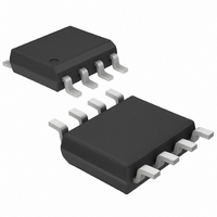
MAX1951ESA+T Maxim Integrated Products, MAX1951ESA+T Datasheet - Page 7

MAX1951ESA+T
Manufacturer Part Number
MAX1951ESA+T
Description
IC REG PWM 2A 8-SOIC
Manufacturer
Maxim Integrated Products
Type
Step-Down (Buck)r
Datasheet
1.MAX1952ESA.pdf
(15 pages)
Specifications of MAX1951ESA+T
Internal Switch(s)
Yes
Synchronous Rectifier
Yes
Number Of Outputs
1
Voltage - Output
0.8 ~ 5.5 V
Current - Output
2A
Frequency - Switching
1MHz
Voltage - Input
2.6 ~ 5.5 V
Operating Temperature
-40°C ~ 85°C
Mounting Type
Surface Mount
Package / Case
8-SOIC (3.9mm Width)
Power - Output
976mW
Lead Free Status / RoHS Status
Lead free / RoHS Compliant
The MAX1951/MAX1952 high-efficiency switching regula-
tors are small, simple, DC-to-DC step-down converters
capable of delivering up to 2A of output current. The
devices operate in pulse-width modulation (PWM) at a
fixed frequency of 1MHz from a 2.6V to 5.5V input voltage
and provide an output voltage from 0.8V to V
the MAX1951/MAX1952 ideal for on-board postregula-
tion applications. The high switching frequency allows
for the use of smaller external components, and internal
synchronous rectifiers improve efficiency and eliminate
the typical Schottky free-wheeling diode. Using the on-
resistance of the internal high-side MOSFET to sense
switching currents eliminates current-sense resistors,
further improving efficiency and cost. The MAX1951
total output error over load, line, and temperature (0°C
to +85°C) is less than 1%.
PIN NAME
1
2
3
4
5
6
7
8
COMP
PGND
GND
V
REF
FB
LX
IN
CC
Supply Voltage. Bypass V
capacitor to ground and 10Ω resistor to IN.
Reference Bypass. Bypass REF with 0.1µF
capacitor to ground.
Ground
Feedback Input. Connect FB to the output to
regulate using the internal feedback resistor
string (MAX1952). Connect an external resistor-
divider from the output to FB and GND to set
the output to a voltage between 0.8V and V
(MAX1951).
Regulator Compensation. Connect series RC
network from COMP to GND. Pull COMP below
0.17V to shut down the regulator. COMP =
GND when V
Compensation and Shutdown Mode section)
Power Ground. Internally connected to GND.
Keep power ground and signal ground planes
separate.
Inductor Connection. Connect an inductor
between LX and the regulator output.
Power-Supply Voltage. Input voltage range
from 2.6V to 5.5V. Bypass IN with a 10µF (min)
ceramic capacitor to GND and a 10Ω resistor
to V
CC
2A PWM Step-Down DC-to-DC Regulators
_______________________________________________________________________________________
.
Detailed Description
1MHz, All-Ceramic, 2.6V to 5.5V Input,
IN
is less than 2.25V (see the
FUNCTION
Pin Description
CC
with 0.1µF
IN
, making
IN
The MAX1951/MAX1952 step-down converters use a
PWM current-mode control scheme. An open-loop com-
parator compares the integrated voltage-feedback signal
against the sum of the amplified current-sense signal and
the slope compensation ramp. At each rising edge of the
internal clock, the internal high-side MOSFET turns on
until the PWM comparator trips. During this on-time, cur-
rent ramps up through the inductor, sourcing current to
the output and storing energy in the inductor. The current-
mode feedback system regulates the peak inductor cur-
rent as a function of the output voltage error signal. Since
the average inductor current is nearly the same as the
peak inductor current (<30% ripple current), the circuit
acts as a switch-mode transconductance amplifier. To
preserve inner-loop stability and eliminate inductor stair-
casing, a slope-compensation ramp is summed into the
main PWM comparator. During the second half of the
cycle, the internal high-side p-channel MOSFET turns off,
and the internal low-side n-channel MOSFET turns on.
The inductor releases the stored energy as its current
ramps down while still providing current to the output. The
output capacitor stores charge when the inductor current
exceeds the load current, and discharges when the
inductor current is lower, smoothing the voltage across
the load. Under overload conditions, when the inductor
current exceeds the current limit (see the Current Limit
section), the high-side MOSFET does not turn on at the
rising edge of the clock and the low-side MOSFET
remains on to let the inductor current ramp down.
An internal current-sense amplifier produces a current
signal proportional to the voltage generated by the
high-side MOSFET on-resistance and the inductor cur-
rent (R
and the internal slope compensation signal are
summed together into the comparator’s inverting input.
The PWM comparator turns off the internal high-side
MOSFET when this sum exceeds the output from the
voltage-error amplifier.
The internal high-side MOSFET has a current limit of 3.1A
(typ). If the current flowing out of LX exceeds this limit,
the high-side MOSFET turns off and the synchronous
rectifier turns on. This lowers the duty cycle and causes
the output voltage to droop until the current limit is no
longer exceeded. A synchronous rectifier current limit of
-0.6A (typ) protects the device from current flowing into
LX. If the negative current limit is exceeded, the synchro-
nous rectifier turns off, forcing the inductor current to flow
DS(ON)
x I
LX
). The amplified current-sense signal
Controller Block Function
Current Sense
Current Limit
7


