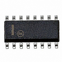
MC34067DWR2G ON Semiconductor, MC34067DWR2G Datasheet - Page 8

MC34067DWR2G
Manufacturer Part Number
MC34067DWR2G
Description
IC CTRLR SMPS DBL END HF 16-SOIC
Manufacturer
ON Semiconductor
Type
Flybackr
Datasheet
1.MC34067DWG.pdf
(16 pages)
Specifications of MC34067DWR2G
Internal Switch(s)
No
Synchronous Rectifier
No
Number Of Outputs
1
Current - Output
100mA
Frequency - Switching
525kHz ~ 2.05MHz
Voltage - Input
2.5 ~ 20 V
Operating Temperature
0°C ~ 70°C
Mounting Type
Surface Mount
Package / Case
16-SOIC (0.300", 7.5mm Width)
Power - Output
862mW
Output Voltage Range
5 V to 5.2 V
Input Voltage Range
20 V
Mounting Style
SMD/SMT
Lead Free Status / RoHS Status
Lead free / RoHS Compliant
Voltage - Output
-
Lead Free Status / Rohs Status
Lead free / RoHS Compliant
Introduction
conversion efficiency and reduce passive component size,
high frequency resonant mode power converters have
emerged as attractive alternatives to conventional
pulse−width modulated control. When compared to
pulse−width modulated converters, resonant mode control
offers several benefits including lower switching losses,
higher efficiency, lower EMI emission, and smaller size.
A new integrated circuit has been developed to support this
trend in power supply design. The MC34067 Resonant
Mode Controller is a high performance bipolar IC dedicated
to variable frequency power control at frequencies
exceeding 1.0 MHz. This integrated circuit provides the
features and performance specifically for zero voltage
switching resonant mode power supply applications.
fixed off−time to the gates of external power MOSFETs at
a repetition rate regulated by a feedback control loop.
Additional features of the IC ensure that system startup and
fault conditions are administered in a safe, controlled manner.
page, which identifies the main functional blocks and the
block−to−block interconnects. Figure 14 is a detailed
functional diagram which accurately represents the internal
circuitry. The various functions can be divided into two
sections. The first section includes the primary control path
which produces precise output pulses at the desired
frequency. Included in this section are a variable frequency
Oscillator, a One−Shot, a pulse Steering Flip−Flop, a pair of
power MOSFET Drivers, and a wide bandwidth Error
Amplifier. The second section provides several peripheral
support
undervoltage lockout, soft−start circuit, and a fault detector.
Primary Control Path
through the interaction of the variable frequency Oscillator,
One−Shot timer and Error Amplifier. The Oscillator triggers
the One−Shot which generates a pulse that is alternately
steered to a pair of totem pole output drivers by a toggle
Flip−Flop. The Error Amplifier monitors the output of the
regulator and modulates the frequency of the Oscillator.
High speed Schottky logic is used throughout the primary
control channel to minimize delays and enhance high
frequency characteristics.
Oscillator
are crucial for precise controller performance at high
operating frequencies. In addition to triggering the
One−Shot timer and initiating the output deadtime, the
oscillator also determines the initial voltage for the one−shot
capacitor. The Oscillator is designed to operate at
As power supply designers have strived to increase power
The primary purpose of the control chip is to provide a
A simplified block diagram of the IC is shown on the front
The output pulse width and repetition rate are regulated
The characteristics of the variable frequency Oscillator
functions
including
a
voltage
OPERATING DESCRIPTION
reference,
http://onsemi.com
8
frequencies exceeding 1.0 MHz. The Error Amplifier can
control the oscillator frequency over a 1000:1 frequency
range, and both the minimum and maximum frequencies are
easily and accurately programmed by the proper selection of
external components.
timer is shown in Figure 16. The oscillator capacitor (C
is initially charged by transistor Q1. When C
4.9 V upper threshold of the oscillator comparator, the base
of Q1 is pulled low allowing C
external resistor, (R
(I
lower threshold of the comparator, Q1 turns on and again
charges C
high slew rate of C
comparator make it difficult to control the peak voltage. This
accuracy issue is overcome by clamping the base of Q1
through a diode to a voltage reference. The peak voltage of
the oscillator waveform is thereby precisely set at 5.1 V.
the current flowing out of the Oscillator Control Current
(I
The input of the voltage regulator is tied to the variable
frequency oscillator. The discharge current of the Oscillator
increases by increasing the current out of the I
Resistor R
output to change the I
occurs when the Error Amplifier output is at its low state
with a saturation voltage of 0.1 V at 1.0 mA.
I
external resistor (R
Amplifier output is at its high state of 2.5 V. The minimum
and maximum oscillator frequencies are programmed by the
proper selection of resistor R
C
OSC
T
OSC
OSC
R
The functional diagram of the Oscillator and One−Shot
C
The frequency of the Oscillator is modulated by varying
The minimum oscillator frequency will result when the
OSC
OSC
R
). When the voltage on C
) pin. The I
current is zero, and C
T
C
Figure 16. Oscillator and One−Shot Timer
OSC
charges from 3.6 V to 5.1 V in less than 50 ns. The
OSC
Control Current
Error Amp Output
VFO
I
OSC
One-Shot RC
OSC Charge
Oscillator
.
is used in conjunction with the Error Amp
OSC RC
OSC
R
VFO
10
OSC
1
2
3
6
OSC
pin is the output of a voltage regulator.
OSC
)
OSC
,
). This occurs when the Error
and the propagation delay of the
and the oscillator control current,
OSC
I
OSC
current. Maximum frequency
OSC
Error Amp
Clamp
OSC
One-Shot
OSC
3.1 V
is discharged through the
Q1
V
and R
CC
to discharge through the
falls below the 3.6 V
4.9 V/3.6 V
4.9V/3.6V
VFO
V
D1
ref
Oscillator
OSC
.
V
CC
exceeds the
OSC
OSC
pin.
)


