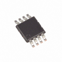
MAX865EUA Maxim Integrated Products, MAX865EUA Datasheet - Page 4

MAX865EUA
Manufacturer Part Number
MAX865EUA
Description
IC DC/DC CONV CHARGE-PUMP 8-UMAX
Manufacturer
Maxim Integrated Products
Type
Switched Capacitor (Charge Pump), Doubler, Invertingr
Datasheet
1.MAX865EUA.pdf
(8 pages)
Specifications of MAX865EUA
Internal Switch(s)
Yes
Synchronous Rectifier
No
Number Of Outputs
2
Voltage - Output
±3.5 ~ ±12 V
Current - Output
20mA
Frequency - Switching
24kHz
Voltage - Input
1.5 ~ 6 V
Operating Temperature
-40°C ~ 85°C
Mounting Type
Surface Mount
Package / Case
8-MSOP, Micro8™, 8-uMAX, 8-uSOP,
Power - Output
330mW
Function
Inverting, Step Up
Output Voltage
- 3 V to - 12 V, 3 V to 12 V
Output Current
20 mA
Maximum Operating Temperature
+ 85 C
Minimum Operating Temperature
- 40 C
Mounting Style
SMD/SMT
Lead Free Status / RoHS Status
Contains lead / RoHS non-compliant
Other names
Q1146982R
Available stocks
Company
Part Number
Manufacturer
Quantity
Price
Company:
Part Number:
MAX865EUA+
Manufacturer:
Maxim
Quantity:
555
Part Number:
MAX865EUA+
Manufacturer:
MAXIM/美信
Quantity:
20 000
Part Number:
MAX865EUA+T
Manufacturer:
MAXIM/美信
Quantity:
20 000
Company:
Part Number:
MAX865EUA-T
Manufacturer:
AD
Quantity:
3 442
Company:
Part Number:
MAX865EUAT
Manufacturer:
MAXIM
Quantity:
6 130
_____________________Pin Description
Compact, Dual-Output Charge Pump
(Circuit of Figure 1, V
4
____________________________Typical Operating Characteristics (continued)
PIN
1
_______________________________________________________________________________________
2
3
4
5
6
7
8
V
IN
= 4.75V, 1mA LOAD
NAME
GND
C2+
C1+
C2-
C1-
V+
V-
IN
(C1 = C2 = C3 = C4 = 1 F)
OUTPUT RIPPLE
IN
Negative Terminal of the Flying Boost
Capacitor
Positive Terminal of the Flying
Inverting Capacitor
Negative Terminal of the Flying
Inverting Capacitor
Output of the Inverting Charge Pump
Ground
Positive Power-Supply Input
Output of the Boost Charge Pump
Positive Terminal of the Flying Boost
Capacitor
= 5V, T
10 s/div
A
= +25°C, unless otherwise noted.)
FUNCTION
V- OUTPUT
20mV/div
V+ OUTPUT
50mV/div
Figure 1. Test Circuit
V
IN
V
3.3 F
3.3 F
IN
= 4.75V, 1mA LOAD
(C1 = C2 = C3 = C4 = 3.3 F)
C1-
C2+
C2-
V-
MAX865
OUTPUT RIPPLE
10 s/div
GND
C1+
V+
IN
3.3 F
3.3 F
V- OUTPUT
10mV/div
V+ OUTPUT
10mV/div
I
I
V
V
+
-
R
R
L
L
+
-
OUT+
OUT-


