LM2596DSADJR4G ON Semiconductor, LM2596DSADJR4G Datasheet - Page 9
LM2596DSADJR4G
Manufacturer Part Number
LM2596DSADJR4G
Description
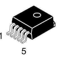
IC REG SW STP-DWN 3A D2PAK-5
Manufacturer
ON Semiconductor
Type
Step-Down (Buck)r
Datasheet
1.LM2596DSADJR4G.pdf
(25 pages)
Specifications of LM2596DSADJR4G
Internal Switch(s)
Yes
Synchronous Rectifier
No
Number Of Outputs
1
Voltage - Output
1.23 ~ 37 V
Current - Output
3A
Frequency - Switching
150kHz
Voltage - Input
4.5 ~ 40 V
Operating Temperature
-40°C ~ 125°C
Mounting Type
Surface Mount
Package / Case
D²Pak, TO-263 (5 leads + tab)
Output Voltage
1.23 V to 37 V
Output Current
3 A
Input Voltage
- 5 V to - 12 V
Switching Frequency
150 KHz
Operating Temperature Range
- 40 C to + 125 C
Mounting Style
SMD/SMT
Duty Cycle (max)
95 %
Lead Free Status / RoHS Status
Lead free / RoHS Compliant
Power - Output
-
Lead Free Status / Rohs Status
Lead free / RoHS Compliant
Available stocks
Company
Part Number
Manufacturer
Quantity
Price
Company:

Part Number:
LM2596DSADJR4G
Manufacturer:
ON
Quantity:
12 400
Part Number:
LM2596DSADJR4G
Manufacturer:
ON/安森美
Quantity:
20 000


PROCEDURE (ADJUSTABLE OUTPUT VERSION: LM2596)
Given Parameters:
1. Programming Output Voltage
2. Input Capacitor Selection (C
3. Catch Diode Selection (D1)
V
V
I
To select the right programming resistor R1 and R2 value (see
Figure 1) use the following formula:
Resistor R1 can be between 1.0 k and 5.0 kW. (For best
temperature coefficient and stability with time, use 1% metal
film resistors).
To prevent large voltage transients from appearing at the input
and for stable operation of the converter, an aluminium or
tantalum electrolytic bypass capacitor is needed between the
input pin +V
located close to the IC using short leads. This capacitor should
have a low ESR (Equivalent Series Resistance) value.
For additional information see input capacitor section in the
“Application Information” section of this data sheet.
A. Since the diode maximum peak current exceeds the
B. The reverse voltage rating of the diode should be at least
Load(max)
out
in(max)
regulator maximum load current the catch diode current
rating must be at least 1.2 times greater than the maximum
load current. For a robust design, the diode should have a
current rating equal to the maximum current limit of the
LM2596 to be able to withstand a continuous output short.
1.25 times the maximum input voltage.
= Regulated Output Voltage
V out + V
= Maximum DC Input Voltage
= Maximum Load Current
in
and ground pin GND This capacitor should be
ref
R2 + R1
1.0 )
Procedure
R2
R1
in
V
V
)
out
ref
where V
* 1.0
ref
= 1.23 V
http://onsemi.com
9
Given Parameters:
1. Programming Output Voltage (selecting R1 and R2)
2. Input Capacitor Selection (C
the input and ground pin provides sufficient bypassing.
3. Catch Diode Selection (D1)
V
V
I
Select R1 and R2:
A 100 mF, 50 V aluminium electrolytic capacitor located near
A. For this example, a 3.0 A current rating is adequate.
B. For robust design use a 30 V 1N5824 Schottky diode or
Load(max)
out
in(max)
R2 = 3.0 kW, choose a 3.0k metal film resistor.
any suggested fast recovery diode in the Table 2.
= 5.0 V
V out + 1.23 1.0 )
R2 + R1
= 12 V
= 3.0 A
V out
V
ref
* 1.0
Example
R2
R1
in
)
+
Select R1 = 1.0 kW
1.23 V
5 V
* 1.0
Related parts for LM2596DSADJR4G
Image
Part Number
Description
Manufacturer
Datasheet
Request
R

Part Number:
Description:
Simple Switcher Power Converter 150 KHZ 3A Step-down Voltage Regulator, Package: to 263, Pin Nb=5
Manufacturer:
National Semiconductor

Part Number:
Description:
ON Semiconductor [VOLTAGE REGULATOR]
Manufacturer:
ON Semiconductor
Datasheet:
Part Number:
Description:
357-036-542-201 CARDEDGE 36POS DL .156 BLK LOPRO
Manufacturer:
ON Semiconductor
Datasheet:
Part Number:
Description:
357-036-542-201 CARDEDGE 36POS DL .156 BLK LOPRO
Manufacturer:
ON Semiconductor
Datasheet:
Part Number:
Description:
357-036-542-201 CARDEDGE 36POS DL .156 BLK LOPRO
Manufacturer:
ON Semiconductor
Datasheet:
Part Number:
Description:
357-036-542-201 CARDEDGE 36POS DL .156 BLK LOPRO
Manufacturer:
ON Semiconductor
Datasheet:
Part Number:
Description:
357-036-542-201 CARDEDGE 36POS DL .156 BLK LOPRO
Manufacturer:
ON Semiconductor
Datasheet:
Part Number:
Description:
357-036-542-201 CARDEDGE 36POS DL .156 BLK LOPRO
Manufacturer:
ON Semiconductor
Datasheet:
Part Number:
Description:
357-036-542-201 CARDEDGE 36POS DL .156 BLK LOPRO
Manufacturer:
ON Semiconductor
Datasheet:
Part Number:
Description:
357-036-542-201 CARDEDGE 36POS DL .156 BLK LOPRO
Manufacturer:
ON Semiconductor
Datasheet:
Part Number:
Description:
357-036-542-201 CARDEDGE 36POS DL .156 BLK LOPRO
Manufacturer:
ON Semiconductor
Datasheet:
Part Number:
Description:
357-036-542-201 CARDEDGE 36POS DL .156 BLK LOPRO
Manufacturer:
ON Semiconductor
Datasheet:
Part Number:
Description:
Manufacturer:
ON Semiconductor
Datasheet:
Part Number:
Description:
Manufacturer:
ON Semiconductor
Datasheet: