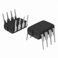
MC34063AP1G ON Semiconductor, MC34063AP1G Datasheet - Page 11

MC34063AP1G
Manufacturer Part Number
MC34063AP1G
Description
IC REG SW DC-DC INV 1.5A 8DIP
Manufacturer
ON Semiconductor
Type
Step-Down (Buck), Step-Up (Boost), Invertingr
Specifications of MC34063AP1G
Internal Switch(s)
Yes
Synchronous Rectifier
No
Number Of Outputs
1
Voltage - Output
1.25 ~ 40 V
Current - Output
1.5A
Frequency - Switching
100kHz
Voltage - Input
3 ~ 40 V
Operating Temperature
0°C ~ 70°C
Mounting Type
Through Hole
Package / Case
8-DIP (0.300", 7.62mm)
Power - Output
1.25W
Output Current
1.5 A
Input Voltage
3 V to 40 V
Switching Frequency
100 KHz
Operating Temperature Range
0 C to + 70 C
Mounting Style
Through Hole
Current, Input Bias
-20 nA
Current, Output
1.5 A
Current, Supply
4 mA
Frequency, Oscillator
33 kHz
Package Type
PDIP-8
Power Dissipation
1.25 W
Regulator Type
DC-DC, Switching
Temperature, Operating, Range
0 to +70 °C
Voltage, Input
-0.3 to +40 VDC
Voltage, Output
40 VDC
Voltage, Supply
40 VDC
Lead Free Status / RoHS Status
Lead free / RoHS Compliant
Other names
MC34063AP1GOS
Available stocks
Company
Part Number
Manufacturer
Quantity
Price
Company:
Part Number:
MC34063AP1G
Manufacturer:
ONSEMI
Quantity:
9 999
Part Number:
MC34063AP1G
Manufacturer:
ON/安森美
Quantity:
20 000
V
V
The following power supply characteristics must be chosen:
V
V
I
f
V
NOTE: For further information refer to Application Note AN920A/D and AN954/D.
out
min
Calculation
out
ripple(pp)
sat
F
in
(t
I
= Forward voltage drop of the output rectifier.
pk(switch)
− Nominal input voltage.
− Desired output current.
on
− Minimum desired output switching frequency at the selected values of V
t
L
= Saturation voltage of the output switch.
− Desired output voltage,
on
R
C
C
(min)
t
t
off
on
+ t
/t
sc
O
T
off
off
− Desired peak−to−peak output ripple voltage. In practice, the calculated capacitor value will need to be increased due to its
)
equivalent series resistance and board layout. The ripple voltage should be kept to a low value since it will directly affect the
line and load regulation.
(V
V out ) V
2I
in(min)
out(max)
I
V
pk(switch)
(t
in(min)
4.0 x 10
9
0.3/I
on
t on ) t
|V
Step−Up
t on
t
V
off
+ t
ripple(pp)
* V sat )
out
I out t on
pk(switch)
F
off
1
f
) 1
| + 1.25 1 ) R2
* V
* V sat
t on
t
) − t
−5
off
off
t
on
off
) 1
in(min)
t
on(max)
Figure 17. Design Formula Table
R1
http://onsemi.com
(V
in(min)
V
I
in(min)
I
pk(switch)
11
pk(switch)
* V sat * V out )
(t
4.0 x 10
0.3/I
Step−Down
on
8V
2I
V out ) V
t on ) t
t on
t
off
+ t
out(max)
* V sat * V out
ripple(pp)
pk(switch)
1
off
f
(t on ) t
) 1
in
−5
) − t
and I
off
t
on
off
F
O
.
off
)
t
on(max)
(V
2I
in(min)
I
out(max)
pk(switch)
Voltage−Inverting
(t
|V out | ) V
4.0 x 10
9
0.3/I
V
on
t on ) t
in
V
t on
t
* V sat )
off
+ t
ripple(pp)
I out t on
pk(switch)
* V sat
1
off
f
) 1
t on
t
−5
) − t
off
off
t
on
off
) 1
F
t
on(max)


